Photomask for forming a resist pattern and manufacturing method thereof, and resist-pattern forming method using the photomask
- Summary
- Abstract
- Description
- Claims
- Application Information
AI Technical Summary
Benefits of technology
Problems solved by technology
Method used
Image

Examples
Embodiment Construction
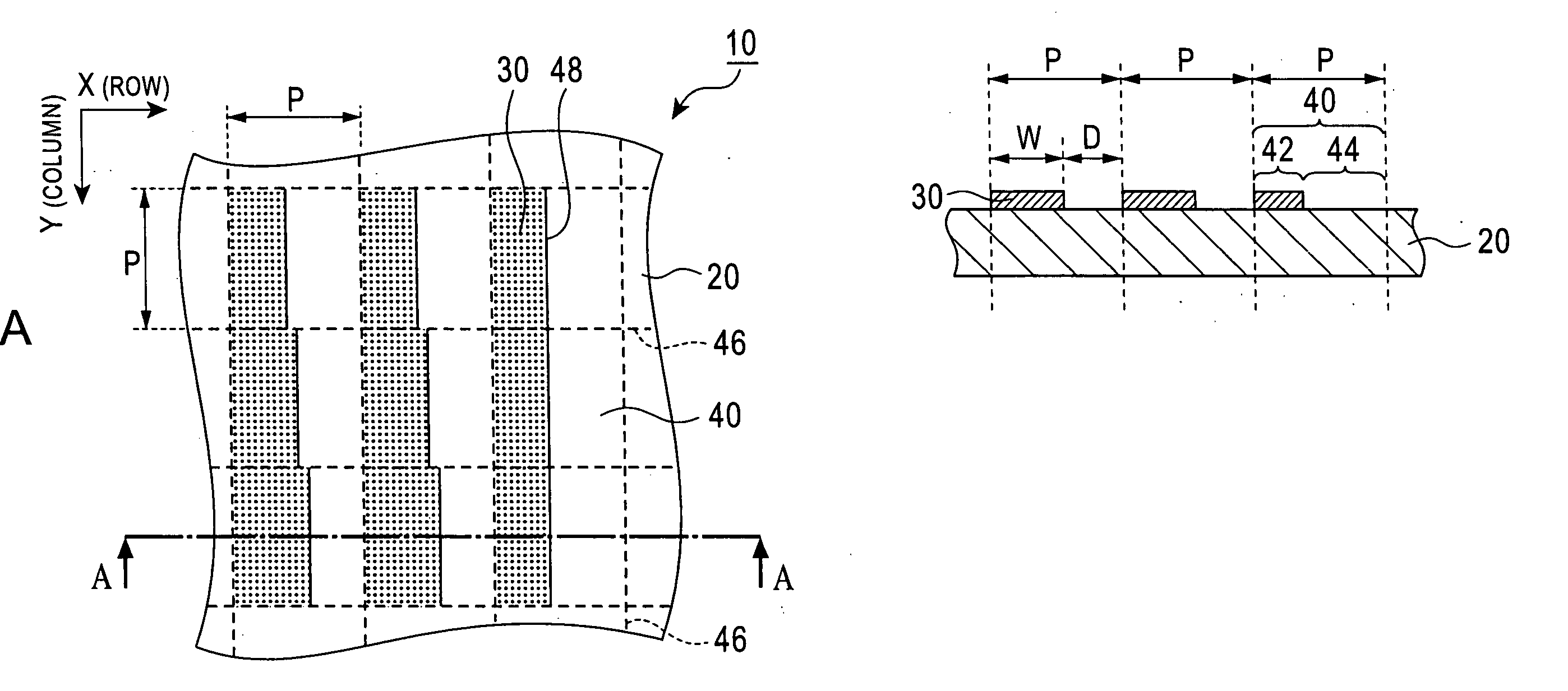
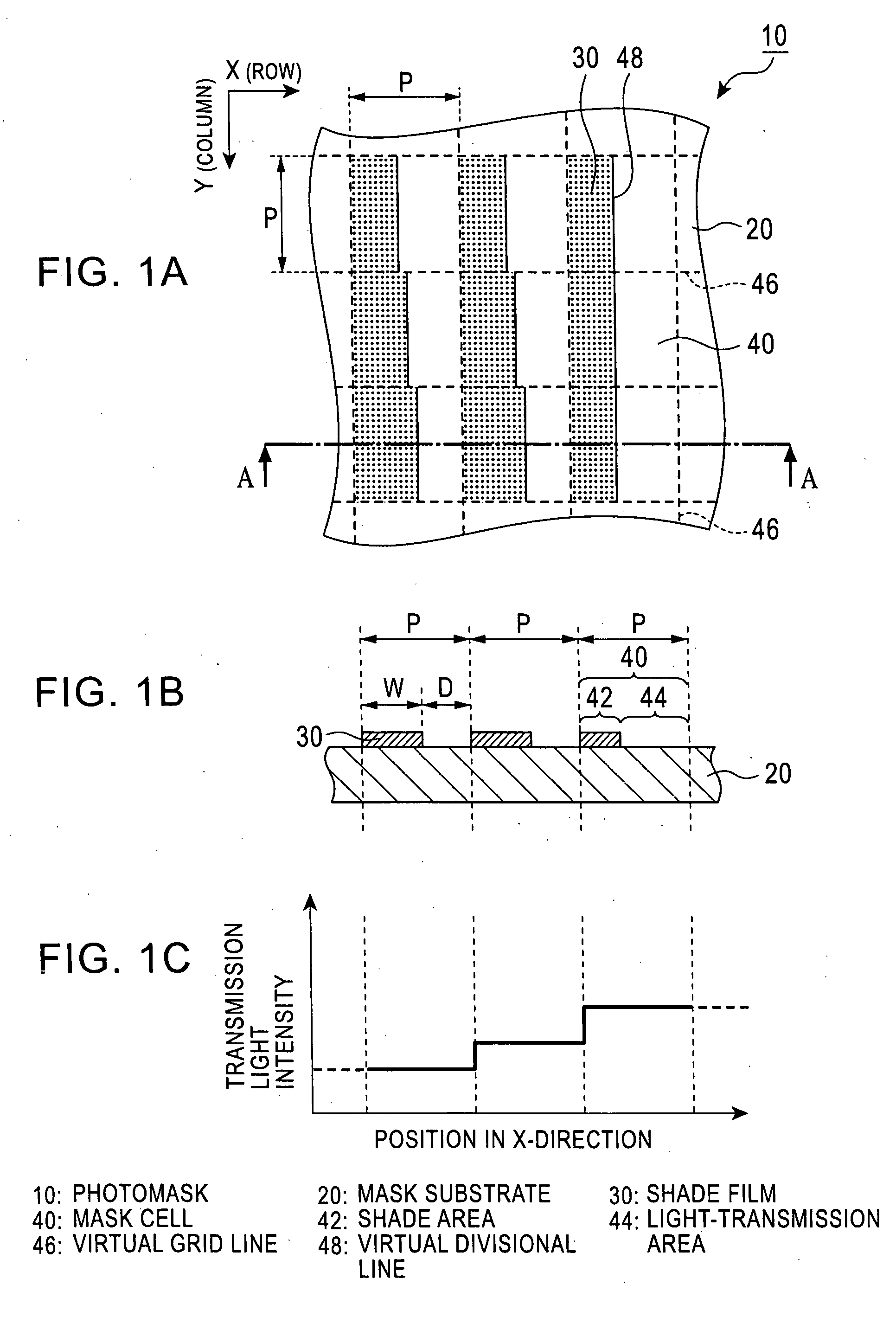
[0053]With reference to the drawings, description will be now made on embodiments of the present invention, wherein constituent elements are schematically shown as to arrangement relationship in a degree to understand the invention. Although preferred embodiments of the invention will be described from now on, the materials and numerical conditions of the elements are mere suitable examples. Therefore, the invention is never limited to the embodiments given in the following. Note that, in the ensuing figures, hatching is partly applied to plan views in order to place emphasis on the required regions thereof, which hatching or the like is not to represent a sectional plane at all.
[0054]Referring to FIGS. 1A-1C, description is now made on a photomask for forming a resist pattern. FIGS. 1A-1C are schematic views illustrating a photomask. FIG. 1A is a plan view of a photomask in a part thereof as viewed from above.
[0055]FIG. 1B is a view showing a section taken along line A-A i...
PUM
 Abstract
Description
Claims
Application Information
 - Generate Ideas
- Intellectual Property
- Life Sciences
- Materials
- Tech Scout
- Unparalleled Data Quality
- Higher Quality Content
- 60% Fewer Hallucinations
Browse by: Latest US Patents, China's latest patents, Technical Efficacy Thesaurus, Application Domain, Technology Topic, Popular Technical Reports.
© 2025 PatSnap. All rights reserved.Legal|Privacy policy|Modern Slavery Act Transparency Statement|Sitemap|About US| Contact US: help@patsnap.com