

Method for forming a stressor structure
a stressor structure and stressor technology, applied in the field of shallow trench isolation stressor structures, can solve the problems of high junction capacitance and junction leakage, difficult to manufacture soi mosfets with strained silicon channels, and inability to meet the requirements of the active silicon layer,
- Summary
- Abstract
- Description
- Claims
- Application Information
AI Technical Summary
Problems solved by technology
Method used
Image

Examples
Embodiment Construction
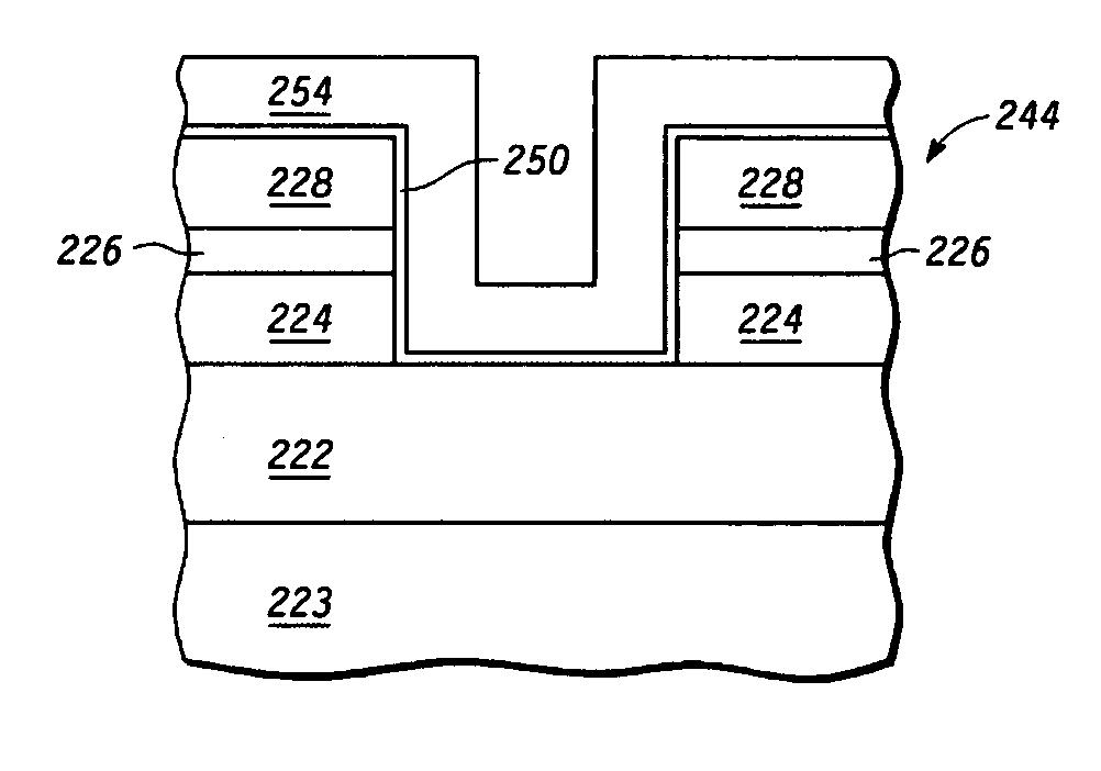
[0024] In one aspect, a method for making a semiconductor device is provided herein. In accordance with the method, a substrate is provided which comprises an active semiconductor layer disposed on a buried dielectric layer. A trench is created in the substrate which exposes a portion of the buried dielectric layer. An oxide layer is formed over the surfaces of the trench, and at least one polysilicon stressor structure is formed over the oxide layer.
[0025] In another aspect, a method for making a semiconductor device is provided. In accordance with the method, a substrate is provided which comprises an active semiconductor layer disposed on a buried dielectric layer. A trench is created in the substrate which exposes a portion of the buried dielectric layer, and a nitride layer is formed over the surfaces of the trench. The trench is backfilled with an oxide, and the oxide is subjected to densification at a maximum densification temperature of less than about 1050° C.
[0026] These...
PUM
 Abstract
Description
Claims
Application Information