Method of repairing process induced dielectric damage by the use of gcib surface treatment using gas clusters of organic molecular species

a surface treatment and organic molecular species technology, applied in the field of methods, can solve the problems of trench and via sidewalls of porous ulk dielectrics, performance degradation of metal contacts, shorting of semiconductor devices, etc., and achieve the effect of reducing the damage of the sidewalls

Inactive Publication Date: 2007-09-27
GLOBALFOUNDRIES INC
View PDF21 Cites 73 Cited by
  • Summary
  • Abstract
  • Description
  • Claims
  • Application Information

AI Technical Summary

Benefits of technology

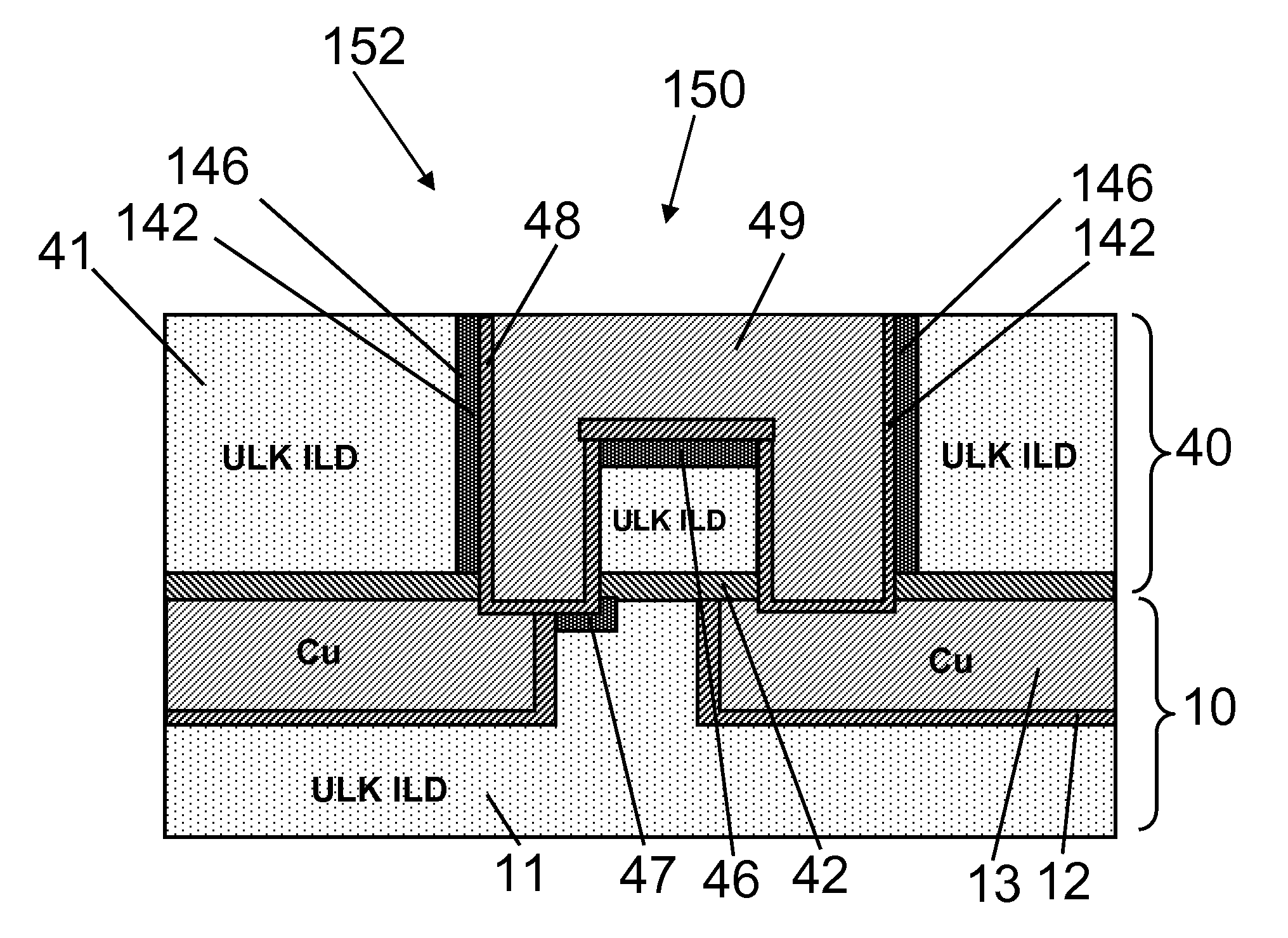
[0006]According to one embodiment of the invention, the size of a typical gas cluster used in the GCIB process may be around, e.g., 5 nm, which is bigger than the size of a typical pore, which is around, e.g., 1˜2 nm, inside a porous ULK material. Therefore, surface treatment by a GCIB process may not cause changes in the property of the bulk ULK material. In the mean time, the GCIB surface treatment may create a smooth layer of densified surface in the ULK dielectric material. According to one embodiment of the invention, the thickness of a densified layer may be controlled preferably by an acceleration voltage used in the GCIB process. According to another embodiment, the thickness of a densified layer may be from 10 Å to 500 Å, and may be preferably in the range of 50 Å-250 Å.
[0007]After the surface treatment through densification, a conventional metallization process may follow by first cleaning the surface of the interconnect structure, and then depositing a metal liner followed by a metal filler in the trench and / or via areas of the interconnect structure. Because the metallization process will now experience a “dense” ILD at the bottom of the trench and / or via, it may not cause roughness to the bottom surface or elements of the metal liner to intrude or penetrate into the underneath porous ULK ILD material. After the build of the interconnect structure is completed, the densified layer may remain inside the porous ILD material. In addition, embodiment of the present invention may enable a dual damascene build for both metal line and via in a porous ULK ILD material.
[0011]Embodiments of the present invention may further provide a method of treating the exposed area of the ILD material by irradiating the exposed area using a GCIB.

Problems solved by technology

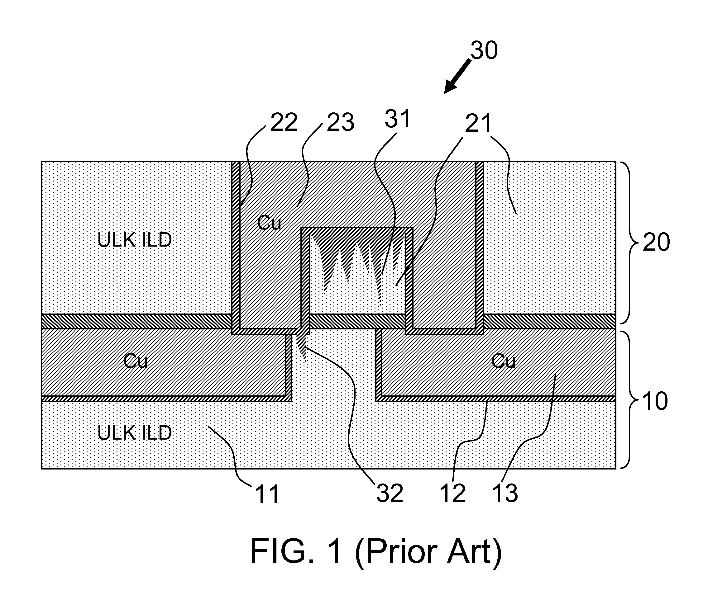
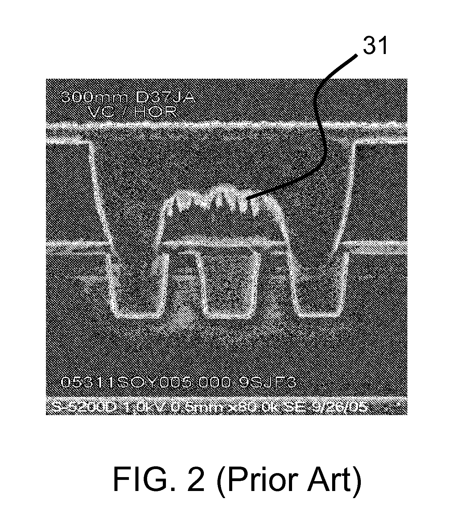
This penetration or intrusion of metal element into porous ULK ILD may cause performance degradation of the metal contacts formed thereon and, in a worst case, shorting of the semiconductor devices that the interconnect structure intends to connect.
In addition to the above-described problems, due to high volume fraction of pores, the trench and via sidewalls of the porous ULK dielectrics are prone to significantly greater damage in the sidewalls relative to the dense low-k dielectrics from the conventional cleaning process, e.g., using oxidative plasma ash chemistries.
Even with these reducing ash chemistries, the damage is significant.
Consequently, in the integration scheme that utilizes a single or dual hardmask approach to protect the underlying ULK dielectric from damage during lithography rework, a large lateral undercut is caused in the ULK dielectric directly below the hardmask during a wet clean process step post-etch.
This undercut presents a challenge for the physical vapor deposition (PVD) of the Cu barrier metal (liner).
Further, the feature profile is modified post-wet etch (damage removal) due to uneven nature of the sidewall damage.
For example, larger damage is observed toward the top of the opening and reduced damage is observed toward the bottom of the opening leading to tapered trench sidewall profiles, impacting the performance.

Method used


Image

  • Method of repairing process induced dielectric damage by the use of gcib surface treatment using gas clusters of organic molecular species
  • Method of repairing process induced dielectric damage by the use of gcib surface treatment using gas clusters of organic molecular species
  • Method of repairing process induced dielectric damage by the use of gcib surface treatment using gas clusters of organic molecular species

Examples


Embodiment Construction

[0041]As is known in the art, manufacture of a semiconductor device may include processing of, for example, a front end of line (FEOL) and a back end of line (BEOL). During a FEOL processing, semiconductor devices such as, for example, switches and logic gates may be produced. These devices may be interconnected through one or more interconnect structures. The interconnect structures may be produced through a BEOL processing.

[0042]A conventional BEOL processing may include steps such as, for example, cap deposition, ILD deposition, hard mask or photo-mask deposition, lithography, and etching, among other steps. For the interest of not obscuring the presentation of the essences of present invention, processing steps that are well known in the art may not be described below in detail, but rather the following description will focus on the distinctive elements of the present invention.

[0043]FIG. 1 is a schematic illustration of an interconnect structure as is known in the art. Intercon...


PUM

PropertyMeasurementUnit
temperatureaaaaaaaaaa
wavelengthaaaaaaaaaa

Abstract

When an interconnect structure is built on porous ultra low k (ULK) material, the bottom and / or sidewall of the trench and / or via is usually damaged by a following metallization or cleaning process which may be suitable for dense higher dielectric materials. Embodiments of the present invention may provide a method of repairing process induced dielectric damage from forming an interconnect structure on an inter-layer dielectric (ILD) material. The method includes treating an exposed area of the ILD material to create a carbon-rich area, and metallizing the carbon-rich area. One embodiment includes providing treatment to an exposed sidewall area of the ILD material to create a carbon-rich area by irradiating the exposed area using a gas cluster ion beam (GCIB) generated through a gas including a straight chain or branched, aliphatic or aromatic hydrocarbon, and metallizing the carbon-rich area.

Description

FIELD OF THE INVENTION[0001]The current invention relates to the field of semiconductor device manufacturing. In particular, it relates to a process of providing treatment to surfaces of an interconnect structure after etching and before metallization.BACKGROUND OF THE INVENTION[0002]Recent rapid advancement in semiconductor technology has brought the advent of very large scale integrated (VLSI) as well as ultra large scale integrated (ULSI) circuitries, resulting in integration of more devices into smaller areas on a single semiconductor substrate. In order to further enhance performance of the VLSI and / or ULSI circuitries, ultra-low dielectric constant (ULK) materials, such as porous materials, are being used as inter-layer dielectric (ILD) to further reduce capacitance such as, for example, inter-layer capacitance and / or other parasitic capacitance that may be undesirable to the performance such as speed of the VLSI and / or ULSI circuitries. Interconnect structures made of metal l...

Claims


Application Information

Patent Timeline
Patent Type & Authority Applications(United States)
IPC IPC(8): H01L21/311
CPCH01L21/3105H01L21/76825H01L21/76808H01L21/31058H01L21/76814H01L21/76831H01L21/31155
Inventor CHEN, SHYNG-TSONGKLYMKO, NANCY R.MADAN, ANITAMEHTA, SANJAYMOLIS, STEVEN E.
Owner GLOBALFOUNDRIES INC
Why Eureka
Try Eureka