Static electricity deflecting device, electron beam irradiating apparatus, substrate processing apparatus, substrate processing method and method of manufacturing substrate

a technology of static electricity and electron beam, which is applied in the field of static electricity deflecting devices, electron beam irradiating apparatus, substrate processing apparatus, and substrate processing methods. it can solve the problems of deterioration of exposure accuracy, material that does not easily discharge static electricity, and tends to be charged up, so as to suppress the occurrence of charge-up and achieve high accuracy

Inactive Publication Date: 2007-10-04
TOKYO ELECTRON LTD
View PDF8 Cites 14 Cited by
  • Summary
  • Abstract
  • Description
  • Claims
  • Application Information

AI Technical Summary

Benefits of technology

[0007]To solve the foregoing problem, a static electricity deflecting device of the present invention includes a cylindrical member having an electron beam passing portion, a plurality of deflecting electrodes which are disposed on an inner wall surface of the cylindrical member along a cylindrical axis thereof and each of which is electrically divided, a plurality of space portions each of which is connected to a gap portion formed by adjacent two of the plurality of deflecting electrodes, each of the plurality of space portions being disposed at an outer position of the gap portion when each of the plurality of space portions is viewed from the electron beam passing portion, and a first conductive film formed in each of the plurality of space portions In the structure of the present invention, of electrons that passed through the electron beam passing portion, electrons that entered a gap portion of adjacent deflecting electrodes enters into a space portion. The electrons are discharged by the first conduction film. Thus, occurrence of charge-up is suppressed. An electron beam emitted by the electron beam irradiating apparatus that has such a static electricity deflecting device is not unnecessarily deflected by charge-up. Thus, the electron beam can be deflected in a desired manner. An exposing device that has such an electron beam irradiating apparatus can perform an exposing process with high accuracy.

Problems solved by technology

Thus, a material that dos not easily discharge static electricity, such as exposed ceramic, tends to be charged up.
As a result, an electron beam is deflected to an undesired position, resulting in deterioration of exposure accuracy.

Method used


Image

  • Static electricity deflecting device, electron beam irradiating apparatus, substrate processing apparatus, substrate processing method and method of manufacturing substrate
  • Static electricity deflecting device, electron beam irradiating apparatus, substrate processing apparatus, substrate processing method and method of manufacturing substrate
  • Static electricity deflecting device, electron beam irradiating apparatus, substrate processing apparatus, substrate processing method and method of manufacturing substrate

Examples


Embodiment Construction

[0096]Next, with reference to the accompanying drawings, embodiments of the present invention will be described.

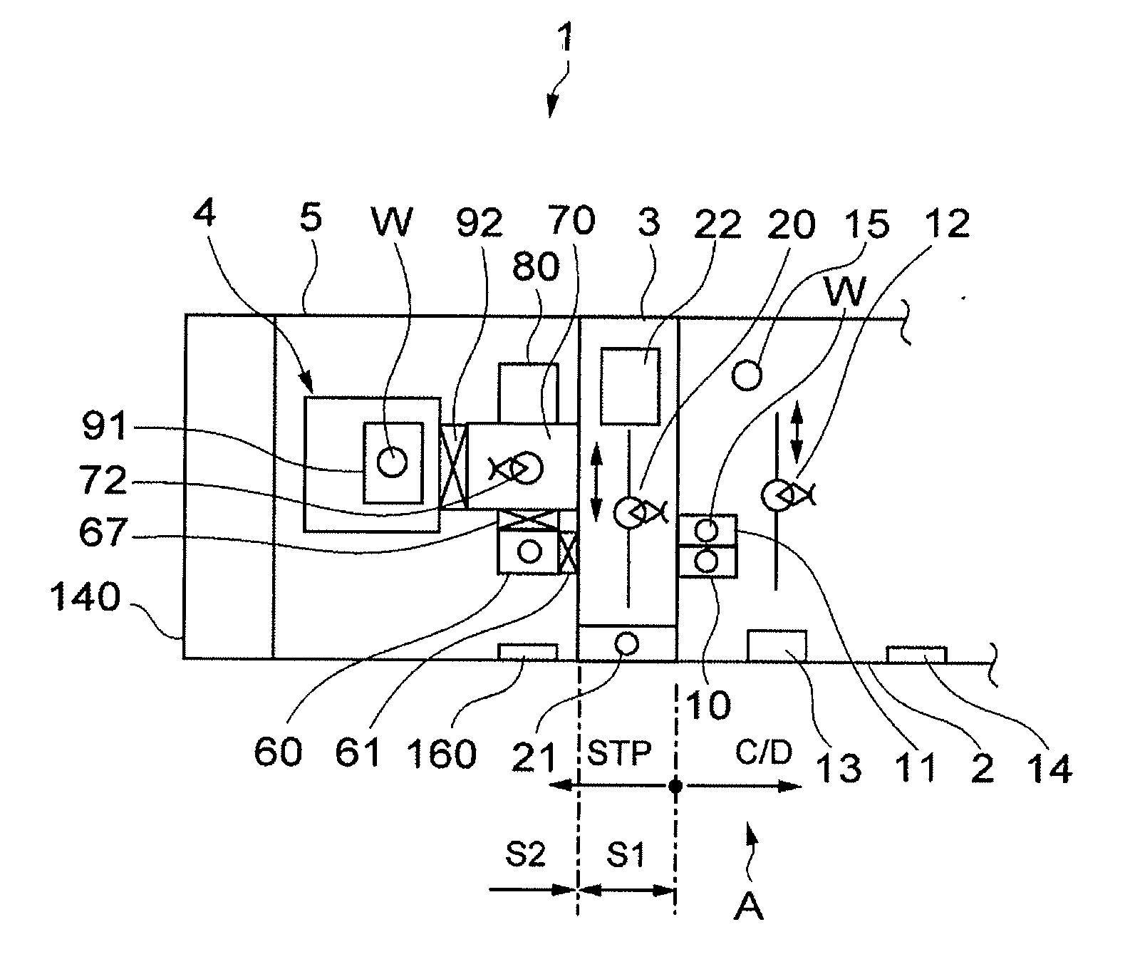
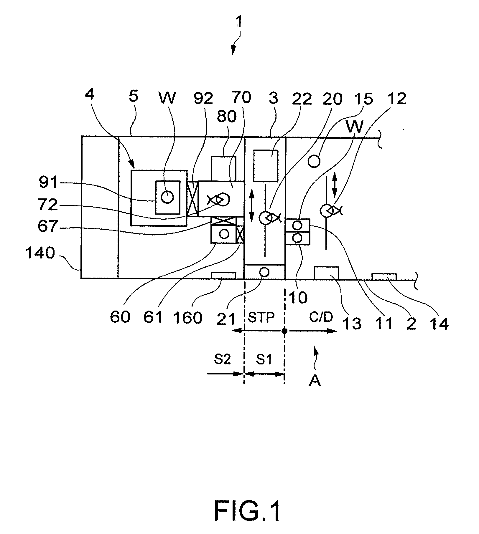
[0097]FIG. 1 is a schematic diagram showing the structure of a system of for example an exposing device as a substrate processing apparatus according to an embodiment of the present invention. The system of the exposing device designated as reference numeral 1 can be freely inline connected to another device, for example a resist processing device 2 (on a C / D side of FIG. 1). The resist processing device 2 has a coating device that coats resist solution on a process surface of a substrate under processing, for example a semiconductor wafer W (the coating device is referred to as a coater (COT)) and a developing device that develops a resist film formed on the process surface of the semiconductor wafer W (the developing device is referred to as a developer (DEV)). The exposing device 1 is composed of an atmospheric aligner section 3 (designated as S1 in FIG. 1) as a first u...


PUM

PropertyMeasurementUnit
volume resistivityaaaaaaaaaa
temperatureaaaaaaaaaa

Abstract

A substrate processing apparatus which irradiates a substrate under processing with an electron beam and processes the substrate with the electron beam is disclosed. The substrate processing apparatus includes an electron beam generation mechanism which generates the electron beam, first area having a plurality of first static electricity deflecting devices whose thicknesses gradually increase in a traveling direction of the electron beam, and a second area disposed on a downstream side of the electron beam of the first area and having a plurality of second static electricity deflecting devices whose thicknesses are nearly same in the traveling direction of the electron beam. The substrate processing apparatus may further include a plurality of lenses whose thicknesses gradually decrease in the traveling direction of the electron beam, at least one of the plurality of lenses being disposed in each of the first area and the second area.

Description

BACKGROUND OF THE INVENTION [0001]1. Field of the Invention[0002]The present invention relates to a static electricity deflecting device, an electron beam irradiating apparatus, a substrate processing apparatus, a substrate processing method, and a method of manufacturing a substrate.[0003]2. Description of the Related Art In recent years, an exposing method using for example an electron beam has been accomplished instead of photolithography technology.[0004]In a conventional exposing apparatus using an electron beam, an objective lens that irradiates a wafer with an electron beam and a static electricity deflecting device that deflects the position of the electron beam on the wafer are disposed in a cylindrical column. In the static electricity deflecting device, a plurality of deflecting electrodes are disposed on an inner wall surface of a base member composed of cylindrical ceramic such that the deflecting electrodes are electrically divided as described in for example Japanese ...

Claims


Application Information

Patent Timeline
Patent Type & Authority Applications(United States)
IPC IPC(8): G21K7/00
CPCB82Y10/00B82Y40/00H01J37/026H01J37/147H01J37/1474H01J37/3174Y10T29/49117H01J2237/151H01L21/67017H01L21/67213Y10T29/49204Y10T29/49885Y10T29/49224H01J2237/03
Inventor FUSE, TAKASHIKOTSUGI, TADASHITSUBOI, KYOTAKEYA, KOJI
Owner TOKYO ELECTRON LTD
Why Eureka
Try Eureka