Photoelectric conversion device and semiconductor device

a conversion device and semiconductor technology, applied in semiconductor devices, solid-state devices, electrical devices, etc., can solve problems such as leakage current occurrence and defects, and achieve the effects of reducing power consumption, reducing leakage current, and highly reliable photoelectric conversion

Inactive Publication Date: 2010-08-10
SEMICON ENERGY LAB CO LTD
View PDF22 Cites 11 Cited by
  • Summary
  • Abstract
  • Description
  • Claims
  • Application Information

AI Technical Summary

Benefits of technology

[0011]It is an object of the present invention to prevent an electric field from concentrating on a corner portion of a photoelectric conversion layer, and to manufacture a photoelectric conversion device in which occurrence of leakage current is suppressed.
[0012]In an photoelectric conversion device of the present invention, by removing a part of an upper layer and a middle layer of a photoelectric conversion layer, it is possible to prevent an electric field from concentrating on a corner portion and to suppress leakage current.
[0028]A photoelectric conversion device of the present invention can suppress a leakage current. In accordance with the present invention, a highly reliable photoelectric conversion device which consumes less power can be obtained. Further, electronic devices incorporating such a photoelectric conversion device can have a high reliability.

Problems solved by technology

However, it is known that in the photoelectric conversion device having the structure shown in FIG. 2, a leakage current occurs in some cases where the photoelectric conversion device operates for a long time.
When an electric field concentrates on this crack, defects such as occurrence of leakage current are caused.

Method used


Image

  • Photoelectric conversion device and semiconductor device
  • Photoelectric conversion device and semiconductor device
  • Photoelectric conversion device and semiconductor device

Examples


embodiment

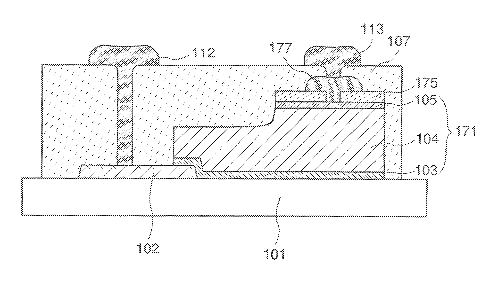
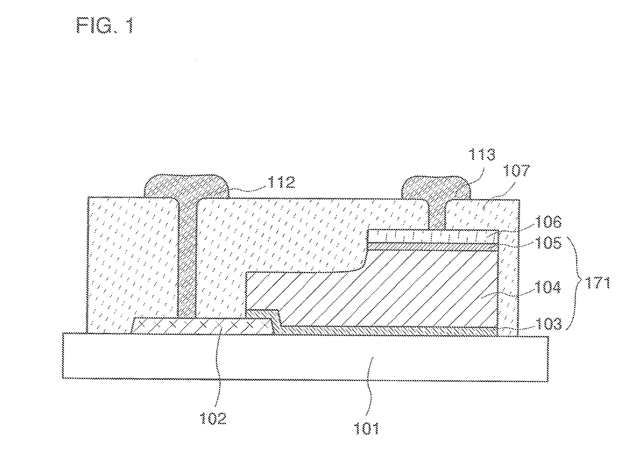
[0053]A photoelectric conversion device of the present invention will be described with reference to FIG. 1, FIGS. 4A to 4C, FIGS. 5A and 5B, and FIGS. 6A and 6B. The present invention is not limited to the following description, and it is easily understood by those skilled in the art that modes and details herein disclosed can be modified in various ways without departing from the spirit and the scope of the present invention. It should be noted that the present invention should not be interpreted as being limited to the description of the embodiment modes to be given below.

[0054]Manufacturing steps of a photoelectric conversion device of the present invention are shown below. A first conductive film 151 is formed over a substrate 101 first (FIG. 4A).

[0055]A flexible substrate is used as the substrate 101, and specifically, a film of polyethylenenaphthalate (PEN) is used. In addition to polyethylenenaphthalate, a film of polyethyleneterephthalate (PET), polybutylenenaphthalate (PBN...

example 1

[0073]In Example 1, a photoelectric conversion device of the present invention is compared with a conventional photoelectric conversion device with reference to FIGS. 23A and 23B.

[0074]In this example, a THB test (Temperature Humidity Bias test) is conducted to evaluate the devices under conditions such as a high temperature of 60° C., a humidity of 90 to 95% and a bias of −5V.

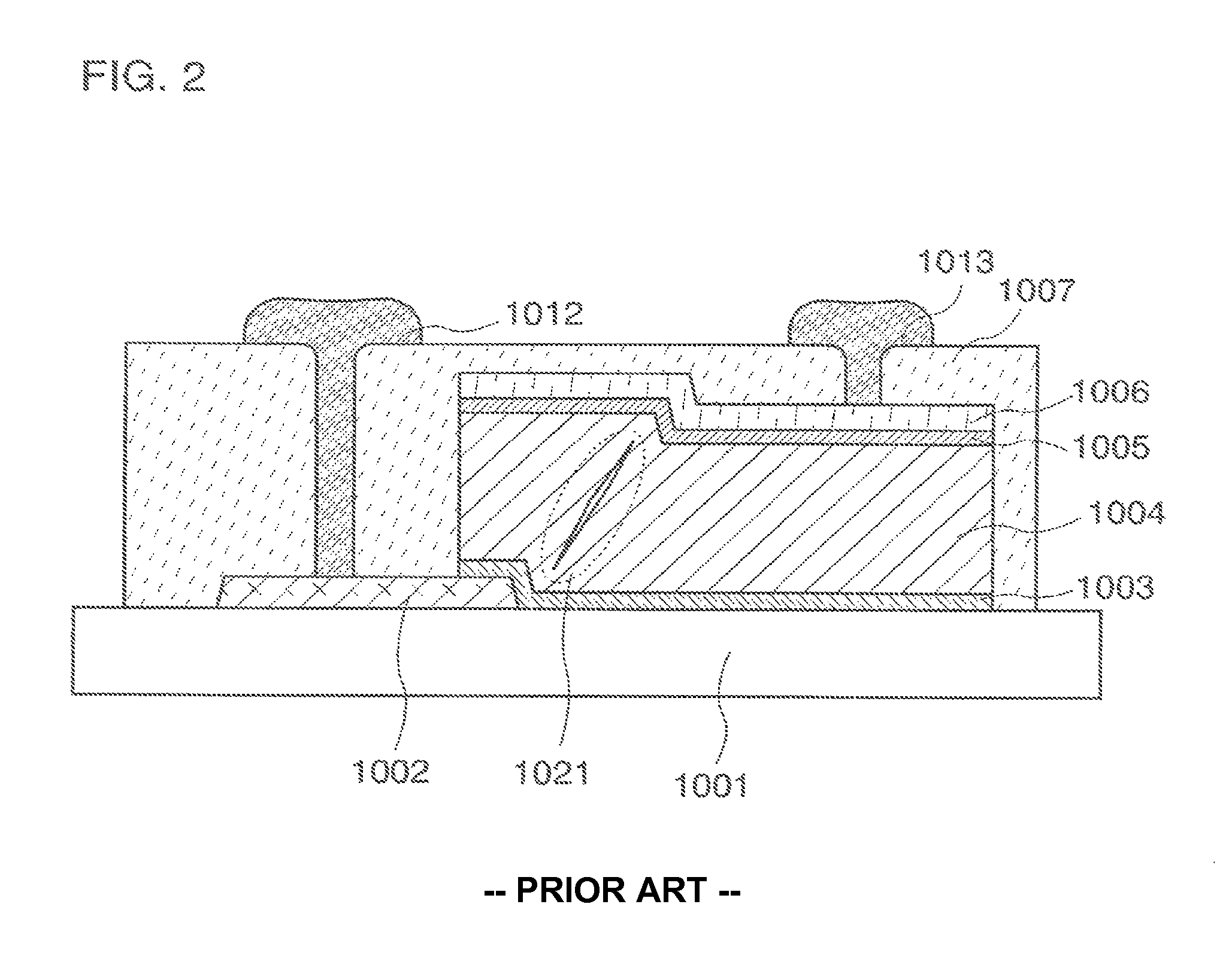
[0075]FIG. 23A shows results of the THB test for the conventional photoelectric conversion device shown in FIG. 2, and FIG. 23B shows results of the THB test for the photoelectric conversion device of the present invention shown in FIG. 1. In addition, in FIGS. 23A and 23B, the horizontal axis represents VL (V) and the vertical axis represents a frequency in each voltage. In addition, VL represents a voltage at which leakage current is generated.

[0076]In the result of 240 hours of the test time, shifts of Vr leakage are seen in both results for the conventional photoelectric conversion device shown in FIG. 2 a...

example 2

[0078]Example 2 describes an example in which an electrode overlapping a photoelectric conversion layer has a structure of stacked films with reference to FIGS. 3A, 3B, 16A and 16B. It should be noted that the same parts as those described in Embodiment are shown by the same reference numerals.

[0079]In this example, an example in which the electrode 102 of FIG. 1 has a three-layer stacked structure is shown in FIGS. 3A, 3B, 16A and 16B. In FIG. 3A, the wiring 131 is made from titanium (Ti), the wiring 132 is made from aluminum (Al), and the wiring 133 is made from titanium (Ti). When the wiring 131 is formed with a transparent electrode, for example, an indium oxide-tin oxide alloy (also referred to as indium tin oxide), or an indium oxide-tin oxide alloy containing silicon (Si) (also referred to as indium tin oxide containing Si) may be used. Besides, zinc oxide (ZnO), tin oxide (SnO2), indium oxide, or an indium oxide-zinc oxide alloy formed by using a target in which indium oxide...


PUM


Abstract

The present invention provides a photoelectric conversion device in which a leakage current is suppressed. A photoelectric conversion device of the present invention comprises: a first electrode over a substrate; a photoelectric conversion layer including a first conductive layer having one conductivity, a second semiconductor layer, and a third semiconductor layer having a conductivity opposite to the one conductivity of the second semiconductor layer over the first electrode, wherein an end portion of the first electrode is covered with the first semiconductor layer; an insulating film, and a second electrode electrically connected to the third semiconductor film with the insulating film therebetween, over the insulating film, are formed over the third semiconductor film, and wherein a part of the second semiconductor layer and a part of the third semiconductor layer is removed in a region of the photoelectric conversion layer, which is not covered with the insulating film.

Description

BACKGROUND OF THE INVENTION[0001]1. Field of the Invention[0002]The present invention relates to a photoelectric conversion device, specifically, a photoelectric conversion device formed using a thin film semiconductor element and a manufacturing method thereof. Further, the present invention relates to electronic devices using a photoelectric conversion device.[0003]2. Description of the Related Art[0004]A number of photoelectric conversion devices generally used for detecting an electromagnetic wave are known, and for example, a photoelectric conversion device having sensitivity in ultra-violet rays to infrared rays are referred to as a photo-sensor in general. A photo-sensor having sensitivity in a visible radiation region with a wave length of 400 nm to 700 nm is particularly referred to as a visible light sensor, and a large number of visible light sensors are used for devices which need illuminance adjustment or on / off control depending on a human living environment.[0005]In p...

Claims


Application Information

Patent Timeline
Patent Type & Authority Patents(United States)
IPC IPC(8): H01L31/075
CPCH01L31/022408H01L31/02162H01L31/1055H01L31/0232H01L31/02325Y02E10/548H01L27/14
Inventor SUGAWARA, YUUSUKENISHI, KAZUOARAO, TATSUYAYAMADA, DAIKITAKAHASHI, HIDEKAZUKUSUMOTO, NAOTO
Owner SEMICON ENERGY LAB CO LTD
Why Eureka
Try Eureka