Semiconductor device and memory card using the same

a technology of semiconductor elements and memory cards, applied in the direction of semiconductor/solid-state device details, electrical apparatus construction details, printed circuit non-printed electric components association, etc., can solve the problems of easy-to-cause characteristic degradation of semiconductor elements, low cutting speed, and inability to machining efficiency down in the cutting step of the circuit board fram

Active Publication Date: 2007-10-04
KIOXIA CORP
View PDF4 Cites 52 Cited by
  • Summary
  • Abstract
  • Description
  • Claims
  • Application Information

AI Technical Summary

Problems solved by technology

However, these machining methods have a problem of a low cutting speed compared with the blade dicing.
When the laser beam machining or the water jet machining is adopted to cut the entire outline, a machining efficiency down in the cutting step of the circuit board frame is unavoidable.
Affected by the heat generated at the time of the cutting, there arise problems such as an insulation performance down between the wirings, a short circuit caused by carbonized resist or core material composing the circuit board, and further an easily-caused characteristic degradation of the semiconductor element.

Method used


Image

  • Semiconductor device and memory card using the same
  • Semiconductor device and memory card using the same
  • Semiconductor device and memory card using the same

Examples


Embodiment Construction

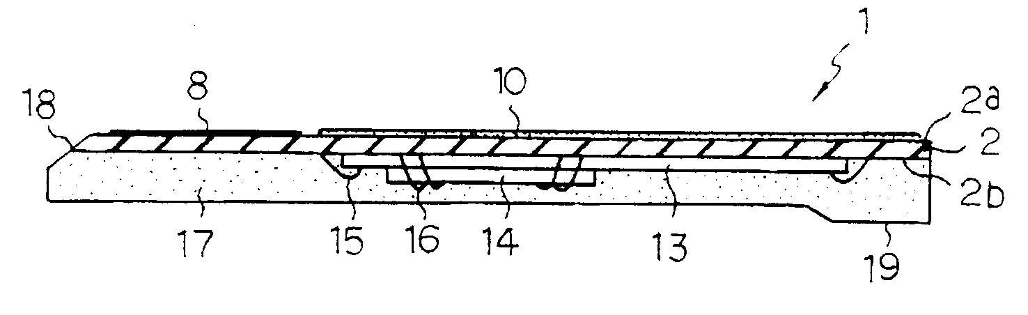
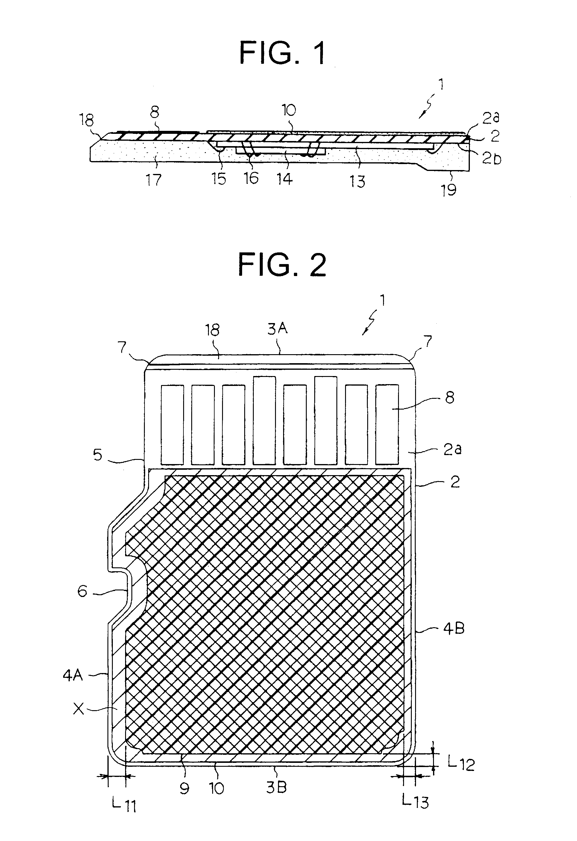
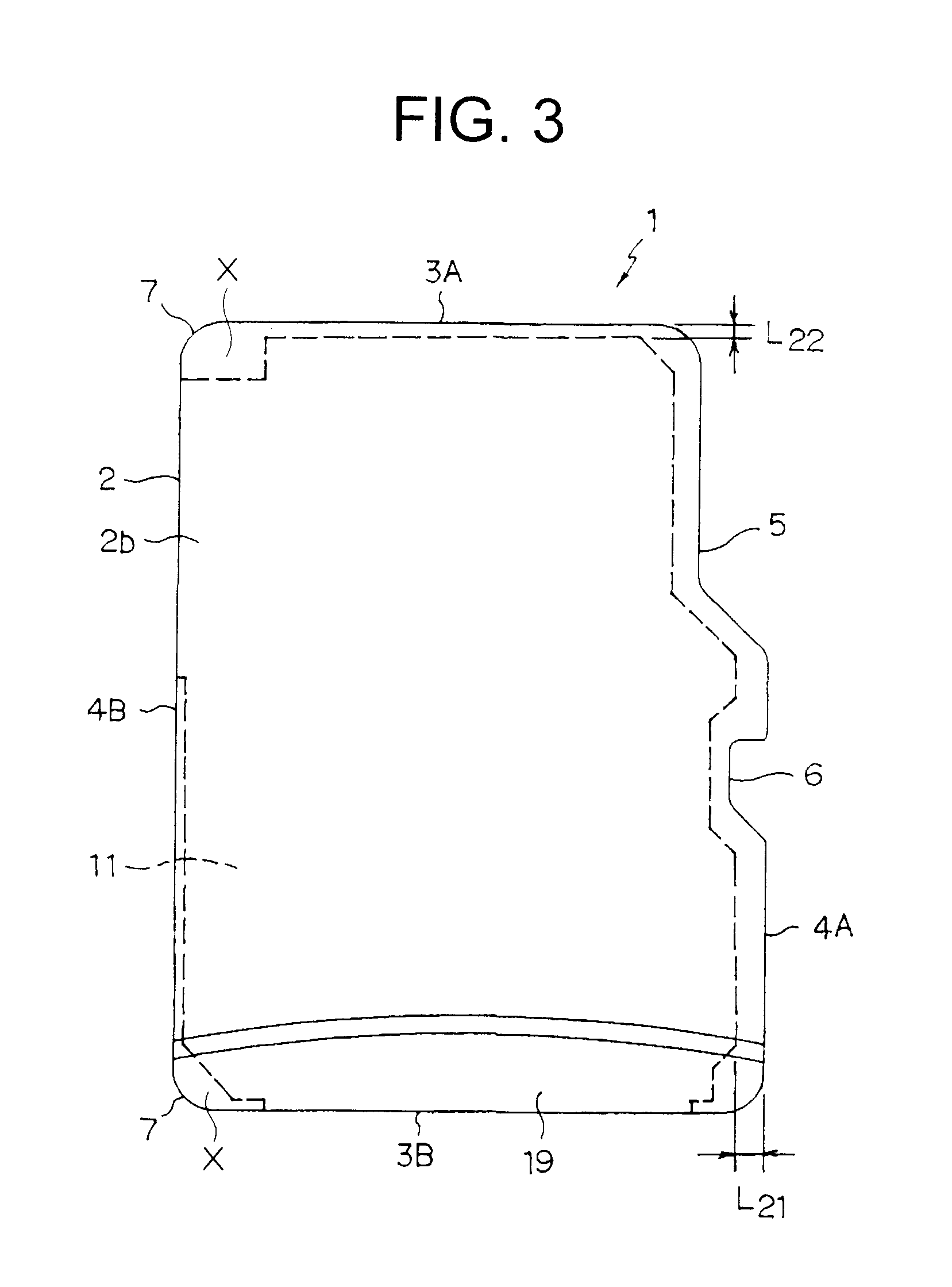
[0022]Hereinafter, a mode to embody the present invention will be described with reference to the drawings. FIG. 1, FIG. 2 and FIG. 3 are views showing a structure of a semiconductor device according to an embodiment of the present invention, in which FIG. 1 is a sectional view of the semiconductor device, FIG. 2 is a plan view (upper view) thereof and FIG. 3 is a rear view thereof. A semiconductor device 1 shown in these view is composed of a memory card, and the semiconductor device 1 is used by itself as, for example, a micro SD™ standard memory card (microSD™ card). The semiconductor device 1 includes a circuit board 2 serving as a terminal forming substrate and an element mounting substrate.

[0023]The circuit board 2 is formed, for example, by providing a wiring network inside or on a surface of an insulating resin substrate, and specifically, a print circuit board using glass epoxy resin, BT resin (Bsmaleimide-Triazine resin) or the like is applicable. The circuit board 2 inclu...


PUM


Abstract

A circuit board has a curved portion provided in at least one side of an external shape thereof. An external connecting terminal is provided on a first main surface of the circuit board. A semiconductor element is mounted on a second main surface of the circuit board. A first wiring network is provided in a region except the terminal region on the first main surface. A second wiring network is provided on the second main surface. Distance from the side including the curved portion to the first wiring network is larger than distance from at least one of the other sides to the first wiring networks, and distance from the side including the curved portion to the second wiring network is larger than distance from at least one of the other sides to the second wiring networks.

Description

CROSS-REFERENCE TO THE RELATED APPLICATION[0001]This application is based upon and claims the benefit of priority from the prior Japanese Patent Application No. 2006-098271 filed on Mar. 31, 2006 and the prior Japanese Patent Application No. 2006-277884 field on Oct. 11, 2006; the entire contents of which are incorporated herein by reference.BACKGROUND OF THE INVENTION[0002]1. Field of the Invention[0003]The present invention relates to a semiconductor device and a memory card using the same.[0004]2. Description of the Related Art[0005]Semiconductor memory cards having a NAND type flash memory or the like built therein are downsized while having larger capacity. For instance, SD™ memory card is presented in three sizes, a size of a normal SD™ card, a size of a mini SD™ card and a size of a micro SD™ card, in which even the micro SD™ card is expected to have a larger capacity. In an attempt to increase the capacity of the downsized memory card, it is examined and put into practical u...

Claims


Application Information

Patent Timeline
Patent Type & Authority Applications(United States)
IPC IPC(8): H01L29/00
CPCH05K1/0256H05K1/117H05K3/0052H05K2203/0228H05K2201/0761H05K2201/09145H05K2201/09227H05K3/284H01L2224/48091H01L2224/49171H01L2924/181
Inventor OKADA, TAKASHIOKADA, KIYOKAZUONO, AKINORINISHIYAMA, TAKU
Owner KIOXIA CORP
Why Eureka
Try Eureka