

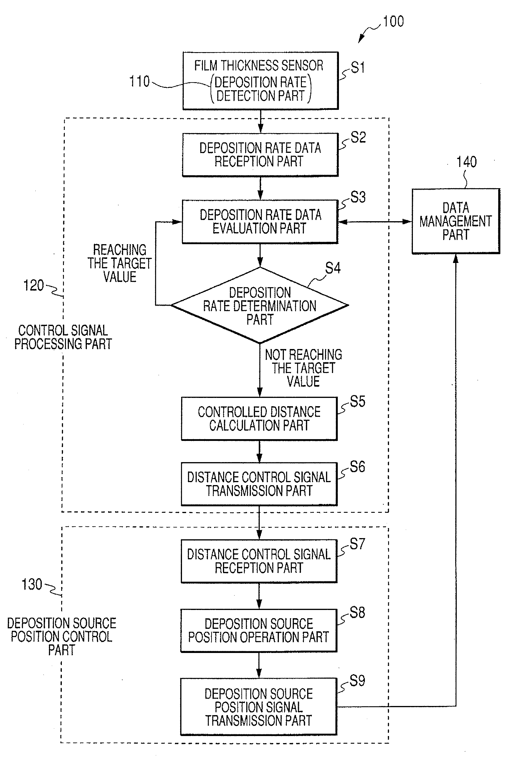
Film formation method
a film and film technology, applied in the direction of vacuum evaporation coating, test/measurement of semiconductor/solid-state devices, coatings, etc., can solve the problems of difficult to obtain constant film thickness distribution, uneven light emission of pixels and substrate surfaces, and yield reduction, etc., to achieve stably obtained constant film thickness distribution
- Summary
- Abstract
- Description
- Claims
- Application Information
AI Technical Summary
Benefits of technology
Problems solved by technology
Method used
Image

Examples
embodiment 1
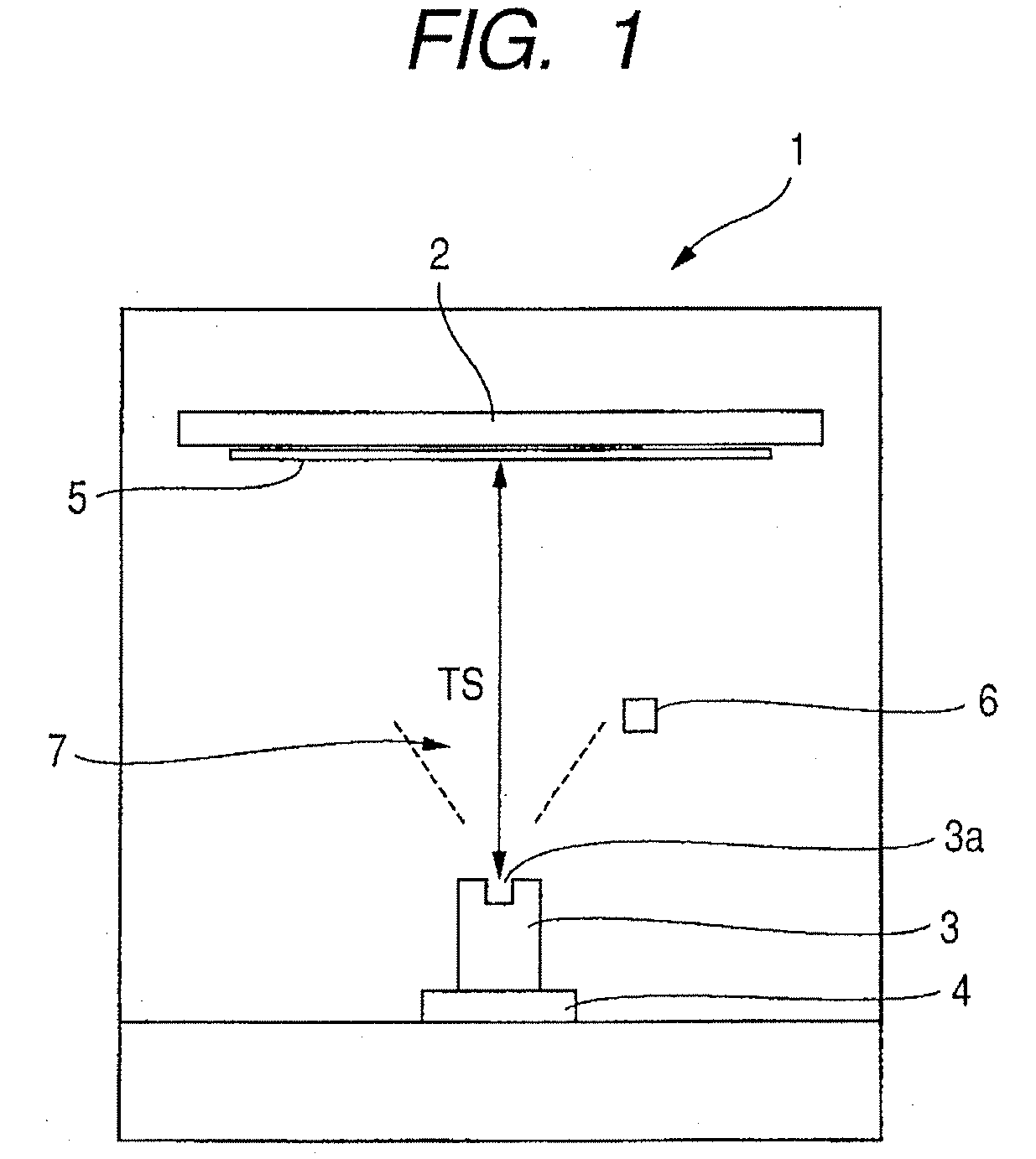
[0081]In the present embodiment, a case where one of organic compound layers constituting an organic electroluminescent device is formed as a film will be described.
[0082]As illustrated in FIG. 3, a substrate holding mechanism 22 for holding a substrate 25 is provided in the upper section of a vacuum chamber 21, and a mask 30 is disposed on the side of a surface which a film is formed of the substrate 25.
[0083]A vapor deposition source position control mechanism 24 for moving a vapor deposition source 23 in the normal direction to the substrate surface is provided in the lower section of the vacuum chamber 21.
[0084]The vapor deposition source is a point source, and the evaporation rate distribution of an evaporation material discharged into an evaporation space conforms to the cosine law.
[0085]The vapor deposition source 23 and the vapor deposition source position control mechanism 24 can be smoothly moved along the longitudinal direction of the substrate 25 in the plane parallel wi...
embodiment 2
[0094]In Embodiment 2, a case where one of organic compound layers constituting an organic electroluminescent device will be described.
[0095]As shown in FIG. 4, for forming a film in the state that a substrate 45 is stood vertically to the ground in a vacuum chamber 41, a substrate holding mechanism 42 for holding the substrate 45 is arranged along a side wall of the vacuum chamber. A mask 50 is disposed on the side of a surface of the substrate 45. Herein, the substrate 45 is held slightly inclined from the vertical surface to the ground by the substrate holding mechanism 42 and a supporting table 48 for making the holding state easily maintained. Two vapor deposition sources 43 and 53 are arranged at positions opposite to the substrate 45.
[0096]Orifices 43a and 53a of the respective vapor deposition sources 43 and 53 have a mechanism by which the orifices 43a and 53a alone move independently. The vapor deposition sources are ones called the valve cell, and have a mechanism by whic...
embodiment 3
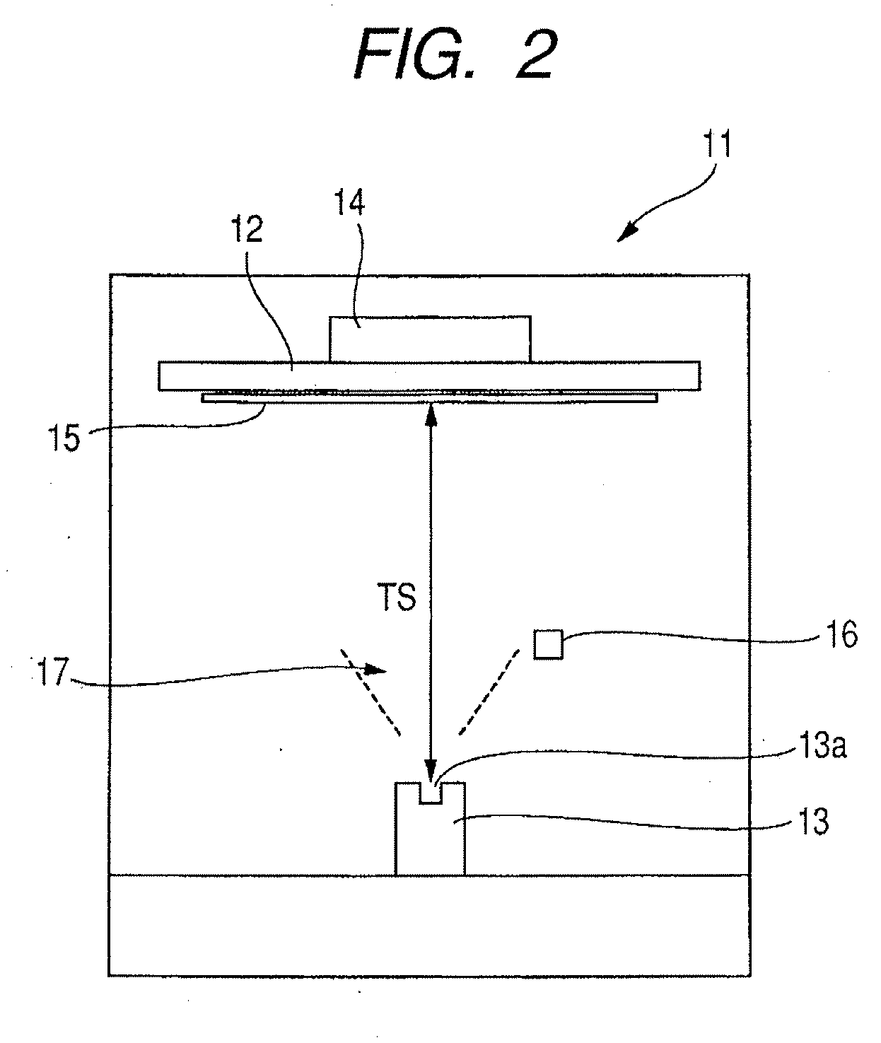
[0103]In Embodiment 3, the separated distance TS is controlled corresponding to change wit elapse of time in pressure inside a vacuum chamber. Hereinafter, a case where one of organic compound layers constituting an organic electroluminescent device is formed as a film will be described.
[0104]A producing apparatus of an organic electroluminescent device shown in FIG. 2 is provided in the upper section thereof with a substrate 15 and a substrate holding mechanism 12 for holding the substrate 15. The substrate holding mechanism 12 is provided with a substrate position control mechanism 14 which can move the substrate 15 along the normal direction to the surface of the substrate 15. A vapor deposition source 13 is arranged in the lower section of the apparatus. A film thickness sensor 16 and a pressure sensor (not shown) are provided in a space between the vapor deposition source 13 and the substrate 15.
[0105]Hereinafter, a case where an organic compound layer is formed as a film using...
PUM
| Property | Measurement | Unit |
|---|---|---|
| pressure | aaaaa | aaaaa |
| temperature | aaaaa | aaaaa |
| pressure | aaaaa | aaaaa |
Abstract
Description
Claims
Application Information