Semiconductor Fabrication Method and Etching System

a technology of etching system and semiconductor, which is applied in the direction of semiconductor/solid-state device manufacturing, electrical equipment, basic electric elements, etc., can solve the problems of difficult to obtain the desired sparse and dense pattern mask dimension, and become difficult to obtain the desired mask dimension and gate electrode dimension in the long term. , to achieve the effect of suppressing fluctuation, good reproducibility and stable obtaining

Inactive Publication Date: 2007-10-04
HITACHI HIGH-TECH CORP
View PDF2 Cites 21 Cited by
  • Summary
  • Abstract
  • Description
  • Claims
  • Application Information

AI Technical Summary

Benefits of technology

[0038] With respect to each target mask dimension shown in Table 1, by performing a deposition step and a trimming step and mutually utilizing the difference between the dimension shift of the sparse mask and the dimension shift of the dense mask of each step, it becomes possible to obtain the desired sparse and dense mask dimensions and gate electrode dimension with good reproducibility.
[0039] Moreover, by detecting the fluctuation quantity of the completely exposed sparse mask dimension and dense mask dimension using a dimension measurement device such as the SEM, and by performing the deposition step and the trimming step while varying at least the gas species, the gas flow rate, the gas pressure, the electrode temperature, the RF bias power or the time so as to suppress the fluctuation, it becomes possible to stably obtain the target sparse and dense mask dimensions and gate electrode dimension.
[0040] In addition, by detecting the fluctuation quantity based on the measurement result of the electrode dimensions of the sparse and dense masks after gate etching, and by determining or correcting the conditions of the deposition step and the trimming step for the subsequent wafer or lot based on the detected information, it becomes possible to suppress long term fluctuation of the sparse gate electrode dimension and dense gate electrode dimension and to stably obtain the target sparse gate electrode dimension and dense gate electrode dimension.

Problems solved by technology

(1) According to the prior art sparse dense control method, the time controllability and the reproducibility were not good, so it was not possible to obtain a desired sparse dense pattern dimension with high accuracy.
(2) In the mass production of a mask pattern in a lithography step, by the fluctuation of dimensions of the completely exposed sparse pattern and dense pattern that vary with time, it becomes difficult to obtain the desired sparse and dense pattern mask dimensions.
(3) By the condition in the reactor of the etching apparatus gradually varying with time, the dimensions of the sparse pattern and dense pattern of the material to be trimmed or material to be etched are also fluctuated, and as a result, it becomes difficult to obtain the desired mask dimension and gate electrode dimension in the long term.

Method used


Image

  • Semiconductor Fabrication Method and Etching System
  • Semiconductor Fabrication Method and Etching System
  • Semiconductor Fabrication Method and Etching System

Examples


embodiment 1

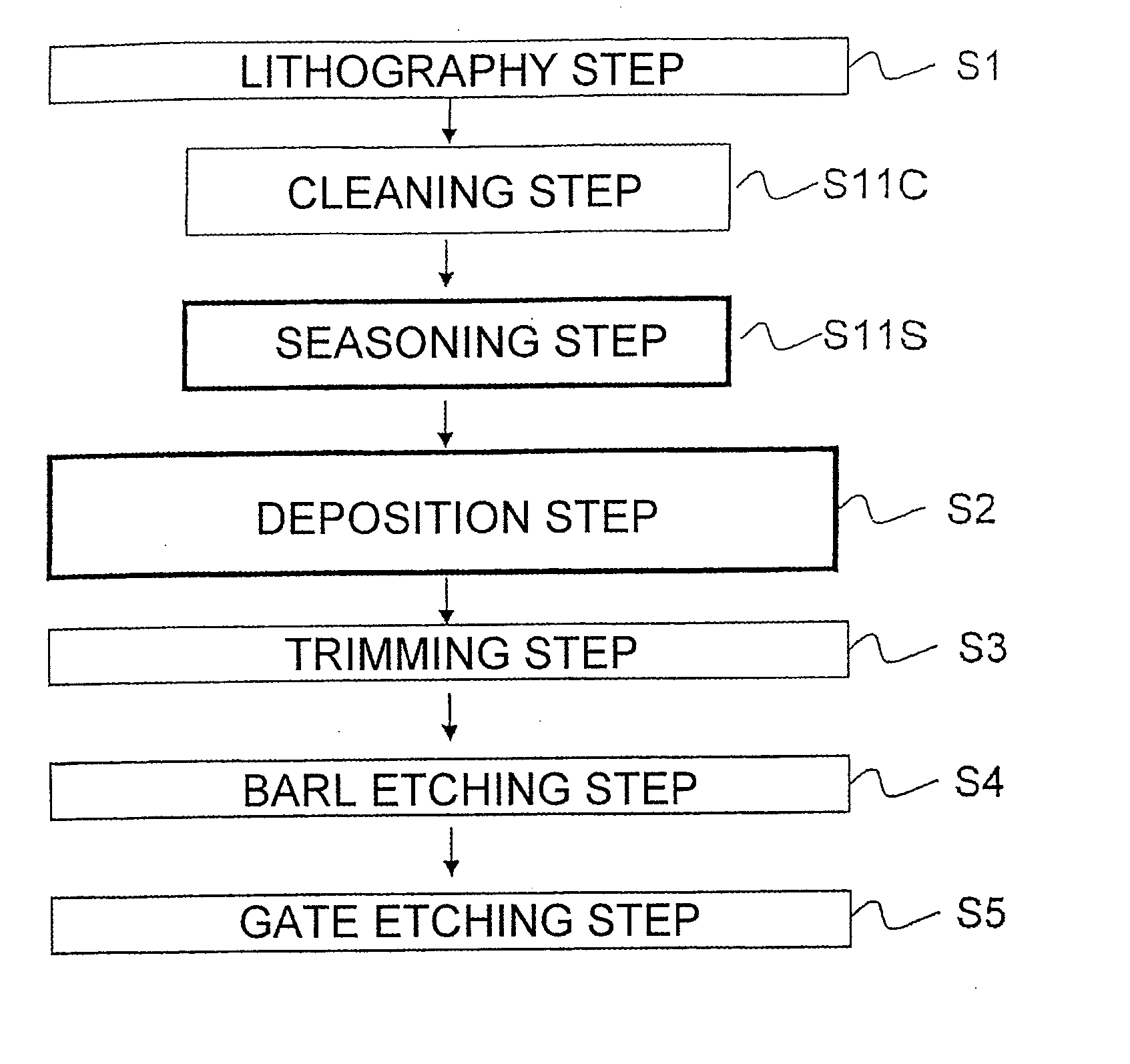
[0066]FIG. 1 is a flowchart showing the process for independently controlling the dimensions of a sparse mask and a dense mask according to the first embodiment of the present invention. The process is described along this flow and with reference to relevant drawings. At first, if sparse and dense mask patterns are formed during a lithography step S1, the result of performing, subsequent to a cleaning step S11C, a seasoning step S11S according to the present invention followed by a deposition step S2 will be described.

[0067] In the seasoning step, a Si wafer is processed under a processing condition in which CHF3 gas is used as deposition gas, the pressure is set to 0.2 Pa, the flow rate is set to 60 ml / min and the RF bias power is set to 5 W. By introducing this seasoning step, prior to starting the deposition step, the status of the wall surface of the apparatus becomes substantially equal to the status thereof during the deposition step. In other words, it is preferable that the...

embodiment 2

[0085] Next, the embodiment regarding the method for controlling the sparse pattern dimension and dense pattern dimension in the deposition step of the present invention shown in FIG. 1 will be described.

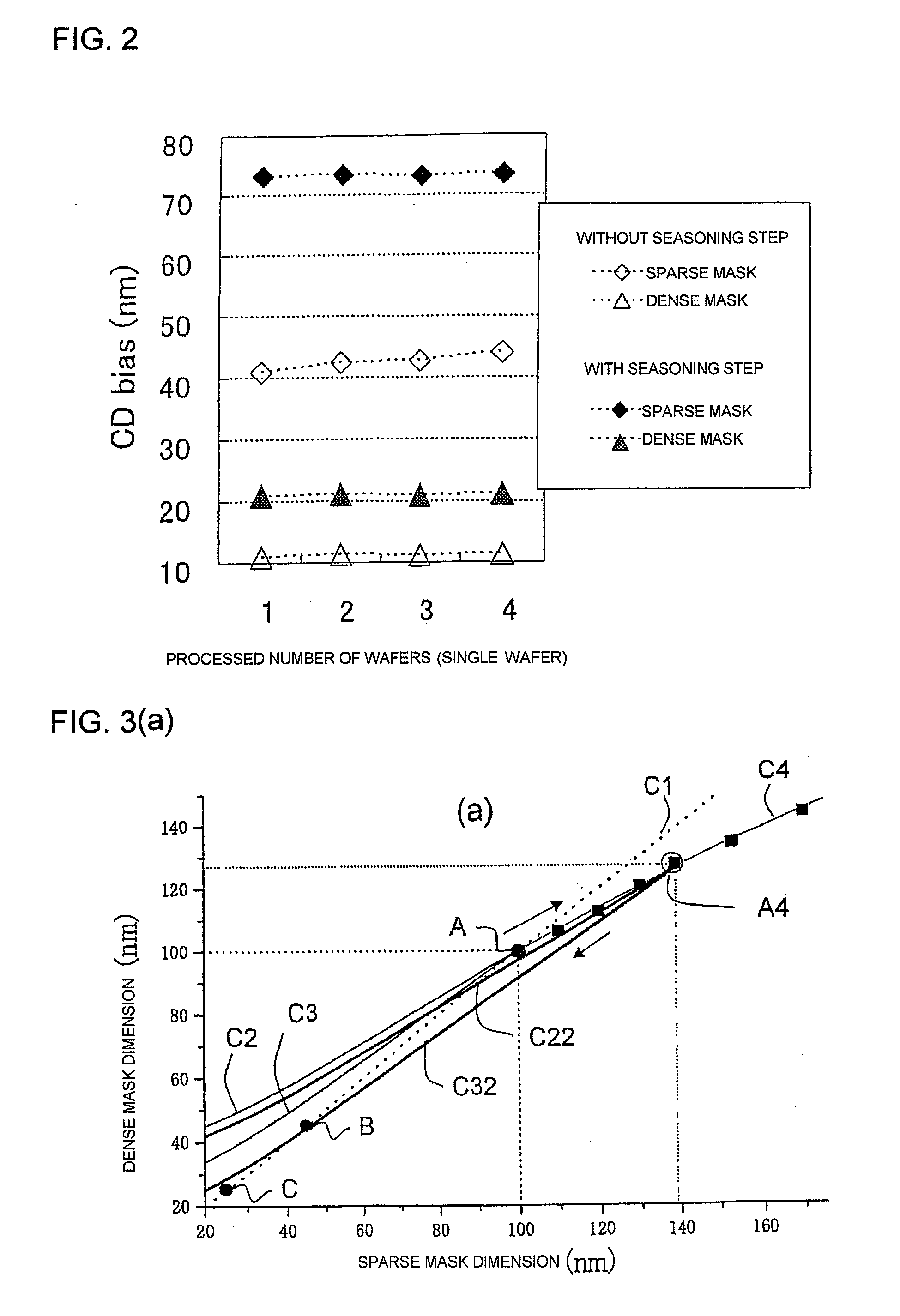
[0086] The gradient of the deposition curve C4 illustrating the time variation of the sparse mask dimension and dense mask dimension described in embodiment 1 can be controlled via apparatus control parameters such as pressure, flow rate, gas species and RF bias power. CHF3 gas is used similarly as embodiment 1, with the pressure set to 2 Pa, the flow rate set to 100 ml / min and the RF bias voltage set to 0 W, and the time variation of the sparse mask and dense mask dimensions is examined. The examination result is shown via triangle plots in FIG. 3(d), and a deposition curve C41 connecting the examination points is drawn, similarly as embodiment 1. As can be seen from this curve, the result of the sparse pattern being wider than the dense pattern is the same as embodiment 1. Howeve...

embodiment 3

[0100] We will now describe an embodiment for stably obtaining a target sparse mask and dense mask dimension with reference to FIG. 9. The present embodiment corresponds to problem (2) to be solved. FIG. 9 is a flowchart according to the second embodiment of the present invention. A step S11 for measuring the dimensions of the sparse mask and dense mask and a step S12 for computing the time for performing the deposition step S2 and the trimming step S3 are added to the process shown in the flowchart of FIG. 1.

[0101] At first, in step S11 for measuring the sparse mask dimension and the dense mask dimension, the fluctuation of the completely exposed sparse mask and dense mask dimensions that vary with time during processing of multiple wafers is detected using OCD (optical critical dimension) or CD-SEM (critical dimension-scanning electron microscope), or CD-AFM (critical dimension-atomic force microscope), or a combination thereof.

[0102] Next, the time for performing the deposition...


PUM


Abstract

The invention provides a semiconductor fabrication method comprising a deposition step for depositing a laminated film on a semiconductor substrate having a region in which a mask pattern is formed sparsely and a region in which the mask pattern is formed densely, a lithography step s1 for forming a mask pattern, a cleaning step S11C for removing deposits in the apparatus, a trimming step S3 for trimming the mask pattern, and dry etching steps S4 and S5 for transferring the mask pattern on the laminated film, wherein a seasoning step S11S followed by a deposition step S2 is introduced either before or after the trimming step S3.

Description

[0001] The present application is based on and claims priorities of Japanese patent application No. 2006-095731 filed on Mar. 30, 2006 and Japanese patent application No. 2007-071122 filed on Mar. 19, 2007, the entire contents of which are hereby incorporated by reference. BACKGROUND OF THE INVENTION [0002] 1. Field of the Invention [0003] The present invention relates to a fabrication method of a semiconductor apparatus including a MOS (metal oxide semiconductor) transistor utilizing electrons or holes as carriers, and especially relates to a dry etching method for stably forming gate electrodes of fine dimension with various pattern densities. [0004] 2. Description of the Related Art [0005] Along with the recent advancement in integration and speed of semiconductor integrated circuits, there are demands for further miniaturization of gate electrodes. However, since even a small fluctuation of dimension of the gate electrode causes the source-drain current or the leak current durin...

Claims


Application Information

Patent Timeline
Patent Type & Authority Applications(United States)
IPC IPC(8): H01L21/302
CPCH01L21/32139H01L21/28123H01L21/3065
Inventor HIROTA, KOUSAMORI, MASAHITOKOFUJI, NAOYUKIITABASHI, NAOSHIMASUDA, TOSHIO
Owner HITACHI HIGH-TECH CORP
Why Eureka
Try Eureka