Radiographic apparatus

a technology of radiographic equipment and beam, which is applied in the direction of radiographic control devices, instruments, television systems, etc., can solve the problems of reducing frame frequency, unstable current flow, and no current flow, and achieve the effect of stably obtaining moving images and high speed

Inactive Publication Date: 2006-05-09
CANON KK
View PDF10 Cites 21 Cited by
  • Summary
  • Abstract
  • Description
  • Claims
  • Application Information

AI Technical Summary

Benefits of technology

[0059]The present invention has been made in consideration of the above-described problems, and has as its object to provide a radiographic apparatus which c

Problems solved by technology

However, if the period of the photoelectric conversion mode becomes too long due to some reason or the illuminance of incident light is high, no current flows in some cases even when light is incident.
When the light incident state changes in this state, the curren

Method used


Image

  • Radiographic apparatus
  • Radiographic apparatus
  • Radiographic apparatus

Examples


first embodiment

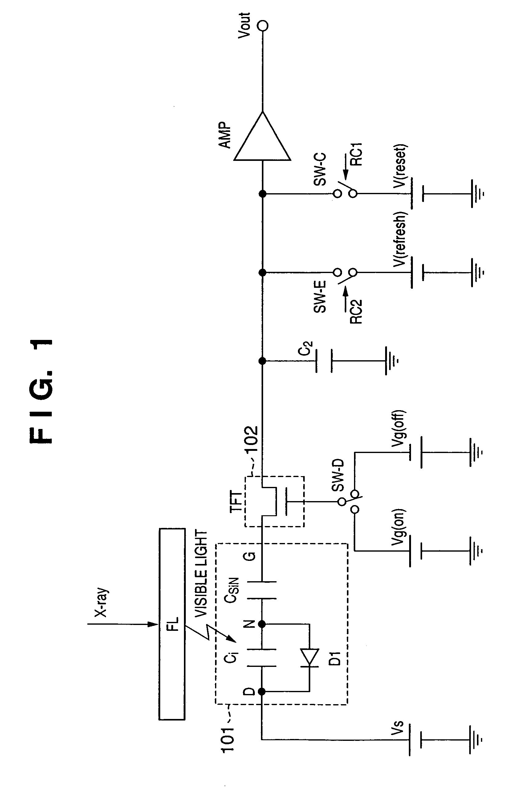
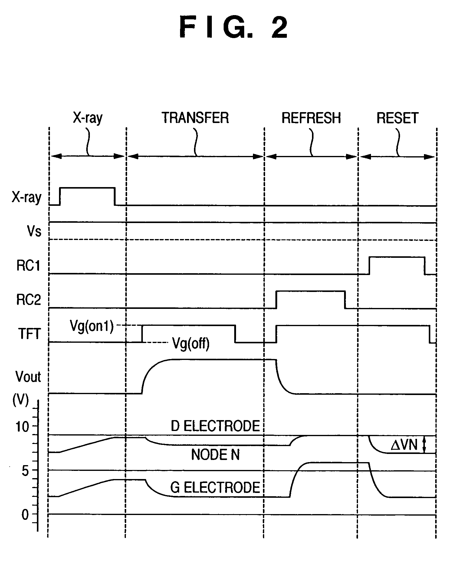
[0097]FIG. 1 is an equivalent circuit diagram of one pixel of an X-ray imaging apparatus according to the first embodiment of the present invention.

[0098]As shown in FIG. 1, a photoelectric conversion element 101 includes a capacitance component Ci formed from an i-layer that is made of, e.g., hydrogenated amorphous silicon and serves as a semiconductor photoelectric conversion layer, and a capacitance component CSiN formed from an insulating layer (an injection inhibiting layer which inhibits injection of carriers of both conductivity types) that is made of, e.g., amorphous silicon nitride. When the photoelectric conversion element 101 is saturated, i.e., no electric field (small electric field) is formed between the D electrode and a node N (in the i-layer), the junction (the node N shown in FIG. 1) between the i-layer and the insulating layer cannot store hole carriers because electrons and holes generated by light recombine.

[0099]That is, the potential of the node N is never hig...

second embodiment

[0143]FIG. 6 is an equivalent circuit diagram of one pixel of an X-ray imaging apparatus according to the second embodiment of the present invention. In the equivalent circuit diagram of the first embodiment shown in FIG. 1, the D electrode of the photoelectric conversion element 101 is biased by the predetermined voltage Vs. In the second embodiment, however, a voltage Vs and voltage Vref can be switched by a switch SW-F.

[0144]As a characteristic feature of this embodiment, the voltage from the G electrode side or that from the D electrode side can be selected as an application voltage to execute the refresh operation of a photoelectric conversion element 101. For example, to acquire one still image, a refresh bias is applied from the D electrode side. That is, an operation based on the timing chart shown in FIG. 28 is executed. On the other hand, to acquire a plurality of still images, a refresh bias is applied from the G electrode side. That is, an operation based on the timing c...

third embodiment

[0151]FIG. 12 is an equivalent circuit diagram of one pixel of an X-ray imaging apparatus according to the third embodiment. The same reference numerals or symbols as in the X-ray imaging apparatus shown in FIG. 1 denote the same component in FIG. 12. Different constituent elements will mainly be described below.

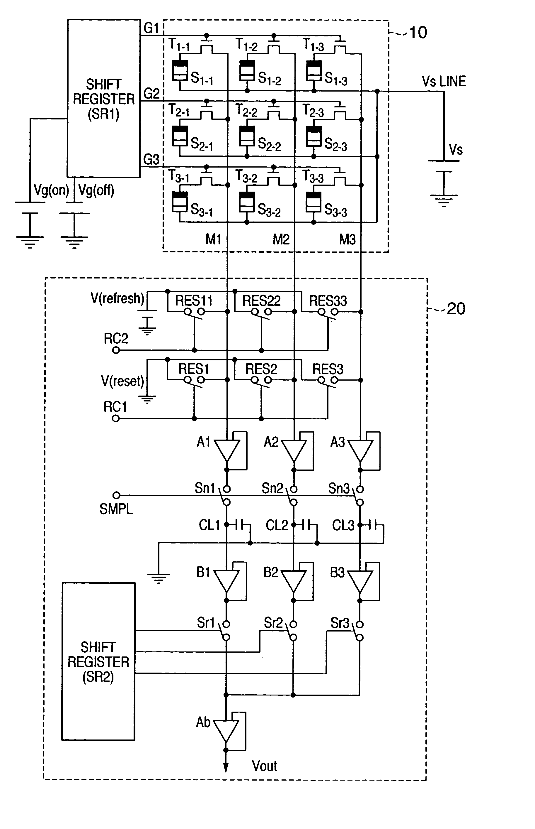
[0152]A switch SW-G shown in FIG. 12 is selectively switched to apply one of a reset bias V(reset) and refresh bias V(refresh) to the noninverting terminal (+) of the operational amplifier (AMP). A capacitive element Cf stores (integrates) a signal current from a photoelectric conversion element 101 through a TFT 102 and is connected between the inverting terminal and an output terminal Vout of the operational amplifier. A switch SW-H is connected in parallel to the capacitive element Cf to reset the integrated signal charges or refresh the photoelectric conversion element 101 through the TFT 102. The switch SW-H is controlled by an RC signal.

[0153]A power supply Vg(on) turn...


PUM


Abstract

An object of this invention is to implement a radiographic apparatus which can stably obtain a moving image at a high speed by suppressing a voltage variation in GND or power supply line and omitting the standby period for each frame. To achieve this object, during a period after electrical signals from conversion elements (S1-1–S1-3) in one control interconnection (G1) are transferred and read for each row by a driving circuit section (SR1) before electrical signals in the next control interconnection are transferred and read, the read-accessed conversion elements are refreshed for each row, thereby eliminating the necessity for preparing a refresh period in acquiring continuous moving images. In addition, since the conversion elements are refreshed for each row, the dark current (transient current) in the refresh mode can be made small as compared to a case wherein all the conversion elements are refreshed at once. With this arrangement, the voltage variation in GND or power supply line is suppressed.

Description

FIELD OF THE INVENTION[0001]The present invention relates to a radiographic apparatus which can suitably be used for medical diagnosis or industrial nondestructive inspection. In this specification, radiation includes electromagnetic waves such as X-rays and γ-rays, or α-rays and β-rays.BACKGROUND OF THE INVENTION[0002]Conventional X-ray imaging systems installed in hospitals and the like can be classified into a film photographing scheme which irradiates a patient with X-rays and exposes the X-rays transmitted through the patient to a film and an image processing scheme which converts X-rays transmitted through a patient into an electrical signal and executes digital image processing.[0003]An example of apparatuses using the image processing scheme is a radiographic apparatus comprising a phosphor which converts X-rays into visible light and a photoelectric conversion device which converts the visible light into an electrical signal. The phosphor is irradiated with X-rays that have...

Claims


Application Information

Patent Timeline
IPC IPC(8): H05G1/64H01L27/14G01T1/17G01T1/20G01T1/208G01T1/24H01L27/146H04N5/30H04N5/32H04N5/335H04N5/361H04N5/374H04N5/376
CPCG01T1/2928H01L27/14658H04N5/32
Inventor ENDO, TADAO
Owner CANON KK
Why Eureka
Try Eureka