High performance transistor with a highly stressed channel

a high-performance, transistor technology, applied in the direction of transistors, semiconductor devices, electrical equipment, etc., can solve the problems of constant effort in the scaling of vlsi circuits and severely degrade transistor performance, and achieve the effect of reducing current crowding effects and high performan

Active Publication Date: 2007-10-04
TAIWAN SEMICON MFG CO LTD
View PDF8 Cites 16 Cited by
  • Summary
  • Abstract
  • Description
  • Claims
  • Application Information

AI Technical Summary

Benefits of technology

[0011] The formation processes of the preferred embodiments of the present invention utilize free surfaces for the development of stress in the cha

Problems solved by technology

The scaling of VLSI circuits is a constant effort.
The current crowding effects result in

Method used


Image

  • High performance transistor with a highly stressed channel
  • High performance transistor with a highly stressed channel
  • High performance transistor with a highly stressed channel

Examples


Embodiment Construction

[0016] The making and using of the presently preferred embodiments are discussed in detail below. It should be appreciated, however, that the present invention provides many applicable inventive concepts that can be embodied in a wide variety of specific contexts. The specific embodiments discussed are merely illustrative of specific ways to make and use the invention, and do not limit the scope of the invention.

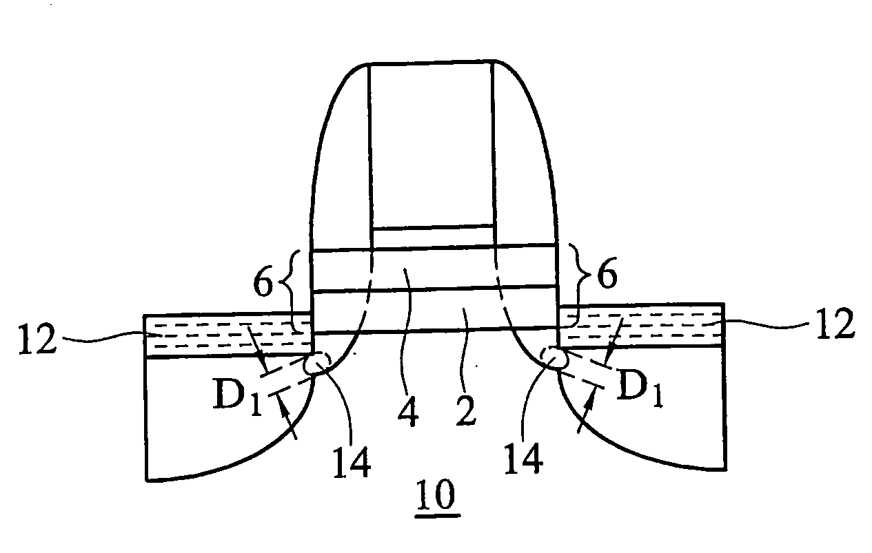
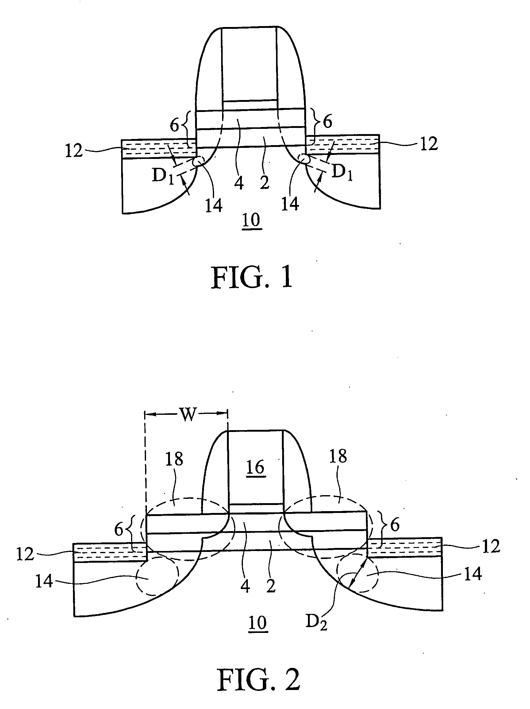
[0017] A possible solution for the problems caused by the scaling of the integrated circuits is shown in FIG. 2, which shows a modified version of the embodiment shown in FIG. 1. The silicon layer 4 and SiGe layer 2 are extended substantially beyond the edges of the gate electrode 16. Therefore, the crowded regions 14 have greater dimensions, and the silicide regions 12 have a greater distance D2 from the substrate 10 than D1 (refer to FIG. 1), so that current crowding effects are reduced. This solution, however, is difficult to implement in the manufacturing processes. Typ...


PUM


Abstract

A MOS transistor having a highly stressed channel region and a method for forming the same are provided. The method includes forming a first semiconductor plate over a semiconductor substrate, forming a second semiconductor plate on the first semiconductor plate wherein the first semiconductor plate has a substantially greater lattice constant than the second semiconductor plate, and forming a gate stack over the first and the second semiconductor plates. The first and the second semiconductor plates include extensions extending substantially beyond side edges of the gate stack. The method further includes forming a silicon-containing layer on the semiconductor substrate, preferably spaced apart from the first and the second semiconductor plates, forming a spacer, a LDD region and a source/drain region, and forming a silicide region and a contact etch stop layer. A high stress is developed in the channel region. Current crowding effects are reduced due to the raised silicide region.

Description

CROSS-REFERENCE TO RELATED APPLICATION [0001] This application is related to commonly assigned U.S. patent application Ser. No. 11 / 115,484, filed Apr. 27, 2005, and entitled “High Performance CMOS Device Design,” which application is incorporated herein by reference.TECHNICAL FIELD [0002] This invention relates generally to semiconductor devices, and more specifically to metal-oxide-semiconductor (MOS) devices having stressed channel regions. BACKGROUND [0003] The scaling of VLSI circuits is a constant effort. With circuits becoming smaller and faster, device driving current improvement becomes more important. Metal-oxide-semiconductor (MOS) transistor current is closely related to gate length, gate capacitance, and carrier mobility. Shortening poly-gate length, increasing gate capacitance and increasing carrier mobility can improve the transistor current performance. Gate length reduction is an ongoing effort in order to shrink circuit size. Increasing gate capacitance has also bee...

Claims


Application Information

Patent Timeline
IPC IPC(8): H01L21/336
CPCH01L29/1054H01L29/665H01L29/6653H01L29/7843H01L29/6659H01L29/66636H01L29/7834H01L29/6656
Inventor WANG, CHIH-HAOTSAI, CHING-WEIWANG, TA-WEI
Owner TAIWAN SEMICON MFG CO LTD
Why Eureka
Try Eureka