Efficient thermoelectric device

a thermoelectric device and efficient technology, applied in the direction of thermoelectric device junction materials, thermoelectric device manufacture/treatment, electrical apparatus, etc., can solve the problems of low efficiency, relegated to a few, rubbed and indefinitely last,

Inactive Publication Date: 2007-10-11
AAMU RES INST
View PDF4 Cites 24 Cited by
  • Summary
  • Abstract
  • Description
  • Claims
  • Application Information

AI Technical Summary

Benefits of technology

[0011]Briefly, the present invention relates to a high efficiency thermo electric device comprising a multi nanolayer structure of alternating insulator and insulator / metal material that is irradiated across the plane of the layer structure with ionizing radiation. The ionizing radiation produces nanocrystals in the layered structure that increase the electrical conductivity and decrease the thermal conductivity thereby increasing the thermoelectric figure of merit. Figures of merit as high as 2.5 have been achieved using layers of co-deposited gold and silicon dioxide interspersed with layers of silicon dioxide. The gold to silicon dioxide ratio was 0.04. 5 MeV silicon ions were used to irradiate the structure. Other metals and insulators may be substituted. Other ionizing radiation sources may be used. The structure tolerates a wide range of metal to insulator ratio.

Problems solved by technology

They are very rugged and can last indefinitely.
Their main shortcoming has been their low efficiency.
The low efficiency relegates TE devices to a few applications where their simplicity and ruggedness outweighs the inefficiency, such as sensors and waste heat energy converters.

Method used


Image

  • Efficient thermoelectric device
  • Efficient thermoelectric device
  • Efficient thermoelectric device

Examples


Embodiment Construction

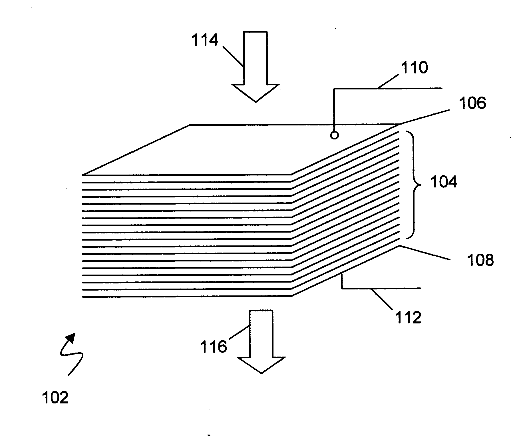
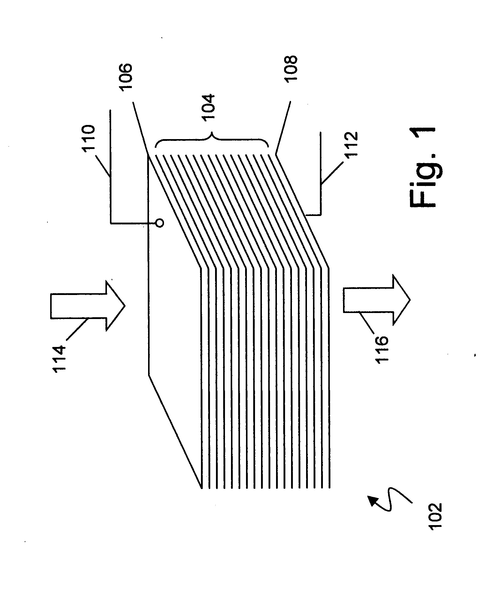
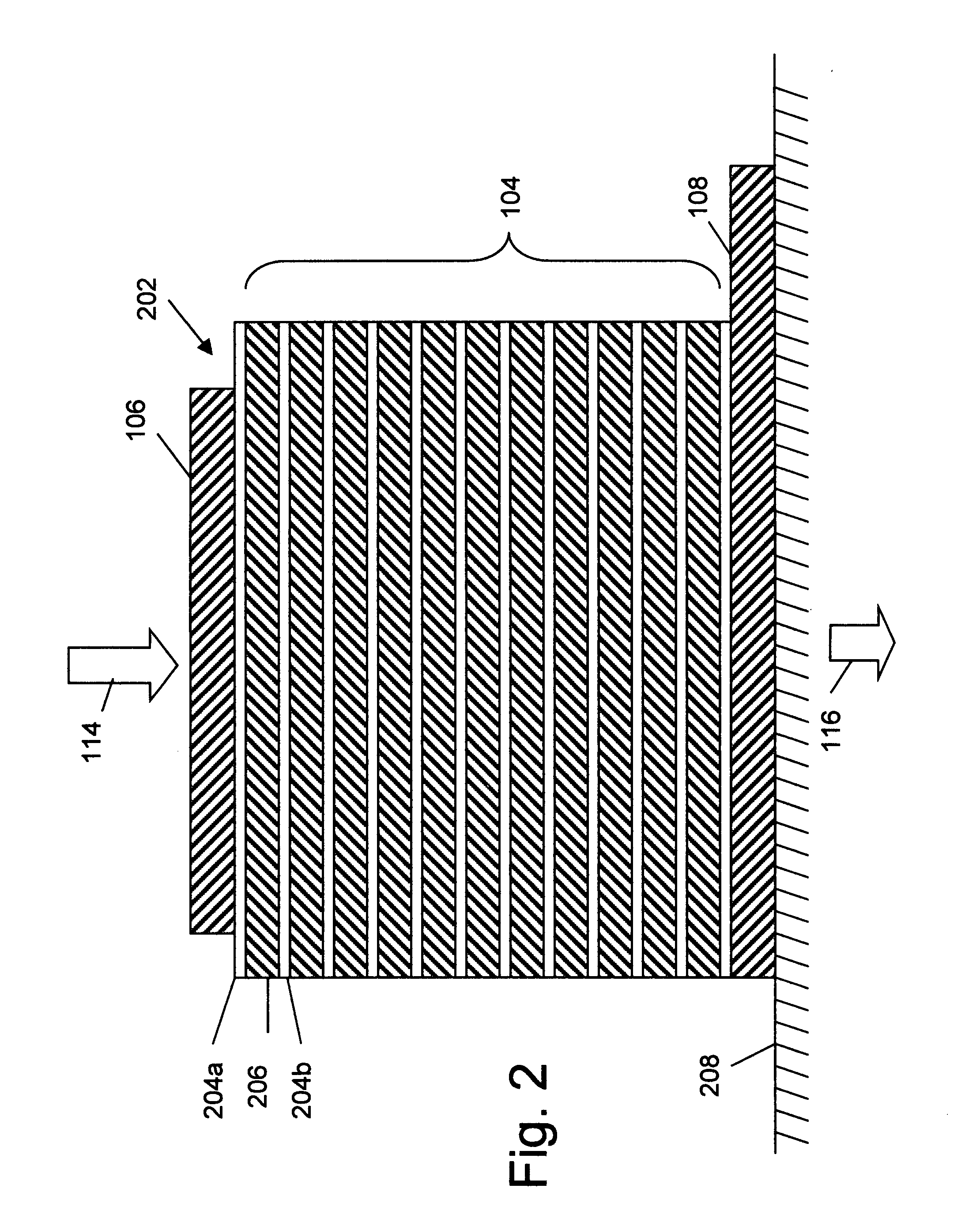
[0027]The present invention achieves high efficiency by building a multilayer structure using alternate layers of insulator and co-deposited metal with insulator, i.e. one layer of insulator followed by a second layer of co-deposited metal with insulator, and then repeat the dual layers 100 to 1000 times or more, as desired. The structure is then irradiated with ionizing radiation to produce nanocrystals of the metal in the co-deposited layers. The irradiation serves to increase the electrical conductivity of the structure, which increases the figure of merit (ZT) and to decrease the thermal conductivity of the structure, further increasing the figure of merit. One exemplary device tested used gold in combination with silicon dioxide.

[0028]Some of the more recent TEG and Peltier prior art devices have been reported to have a figure of merit from below 1 to as high as 2 near room temperature (300° K). However, test devices constructed in accordance with the present invention have dem...


PUM


Abstract

A high efficiency thermo electric device comprising a multi nanolayer structure of alternating insulator and insulator / metal material that is irradiated across the plane of the layer structure with ionizing radiation. The ionizing radiation produces nanocrystals in the layered structure that increase the electrical conductivity and decrease the thermal conductivity thereby increasing the thermoelectric figure of merit. Figures of merit as high as 2.5 have been achieved using layers of co-deposited gold and silicon dioxide interspersed with layers of silicon dioxide. The gold to silicon dioxide ratio was 0.04. 5 MeV silicon ions were used to irradiate the structure. Other metals and insulators may be substituted. Other ionizing radiation sources may be used. The structure tolerates a wide range of metal to insulator ratio.

Description

RELATED APPLICATIONS[0001]This application claims the benefit under 35 USC 119(e) of prior provisional application 60 / 790,612 titled “Efficient Thermoelectric Device,” filed Apr. 10, 2006 by ILA, which is incorporated herein by reference in its entirety.GOVERNMENT RIGHTS[0002]The U.S. Government has a paid-up license in this invention and the right in limited circumstances to require the patent owner to license others on reasonable terms as provided for by the terms of contract number NAG8-1933 from NASA, Huntsville, Ala.BACKGROUND[0003]1. Field of the Invention[0004]The present invention pertains generally to the field of Thermoelectric Devices, more particularly to the field of materials and treatments yielding improved efficiency in thermoelectric devices.[0005]2. Background of the Invention[0006]Thermoelectric (TE) devices convert heat directly to electrical power, or conversely, create heating or cooling directly from electrical power. The devices are entirely solid state, with...

Claims


Application Information

Patent Timeline
Patent Type & Authority Applications(United States)
IPC IPC(8): H01L35/28
CPCH01L35/22H01L35/34H01L35/26H10N10/857H10N10/855H10N10/01
Inventor ILA, DARYUSH
Owner AAMU RES INST
Why Eureka
Try Eureka