Semiconductor device, display device, and electronic device

Inactive Publication Date: 2007-10-11
SEMICON ENERGY LAB CO LTD
View PDF25 Cites 100 Cited by
  • Summary
  • Abstract
  • Description
  • Claims
  • Application Information

AI Technical Summary

Benefits of technology

[0048]By employing the invention, variations of the current value caused by variations in the threshold voltage of a transistor can be suppressed. Therefore, a desired current can be supplied to a load such as a light-e

Problems solved by technology

When the duty ratio is low, the amount of a current supplied to a light-emitting element and a driving transistor is required to be increased, so that a voltage applied to the ligh

Method used


Image

  • Semiconductor device, display device, and electronic device
  • Semiconductor device, display device, and electronic device
  • Semiconductor device, display device, and electronic device

Examples


embodiment mode 1

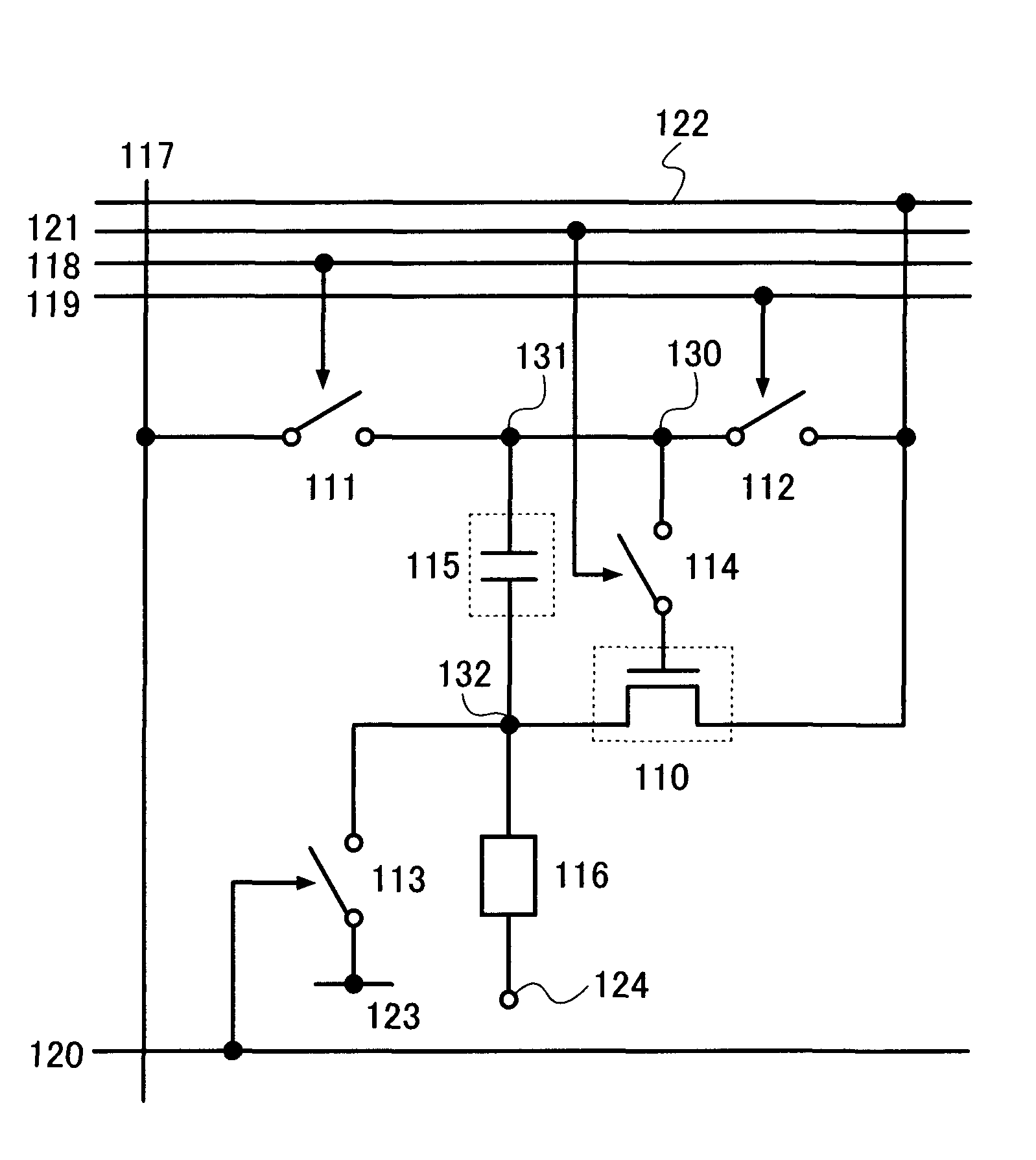
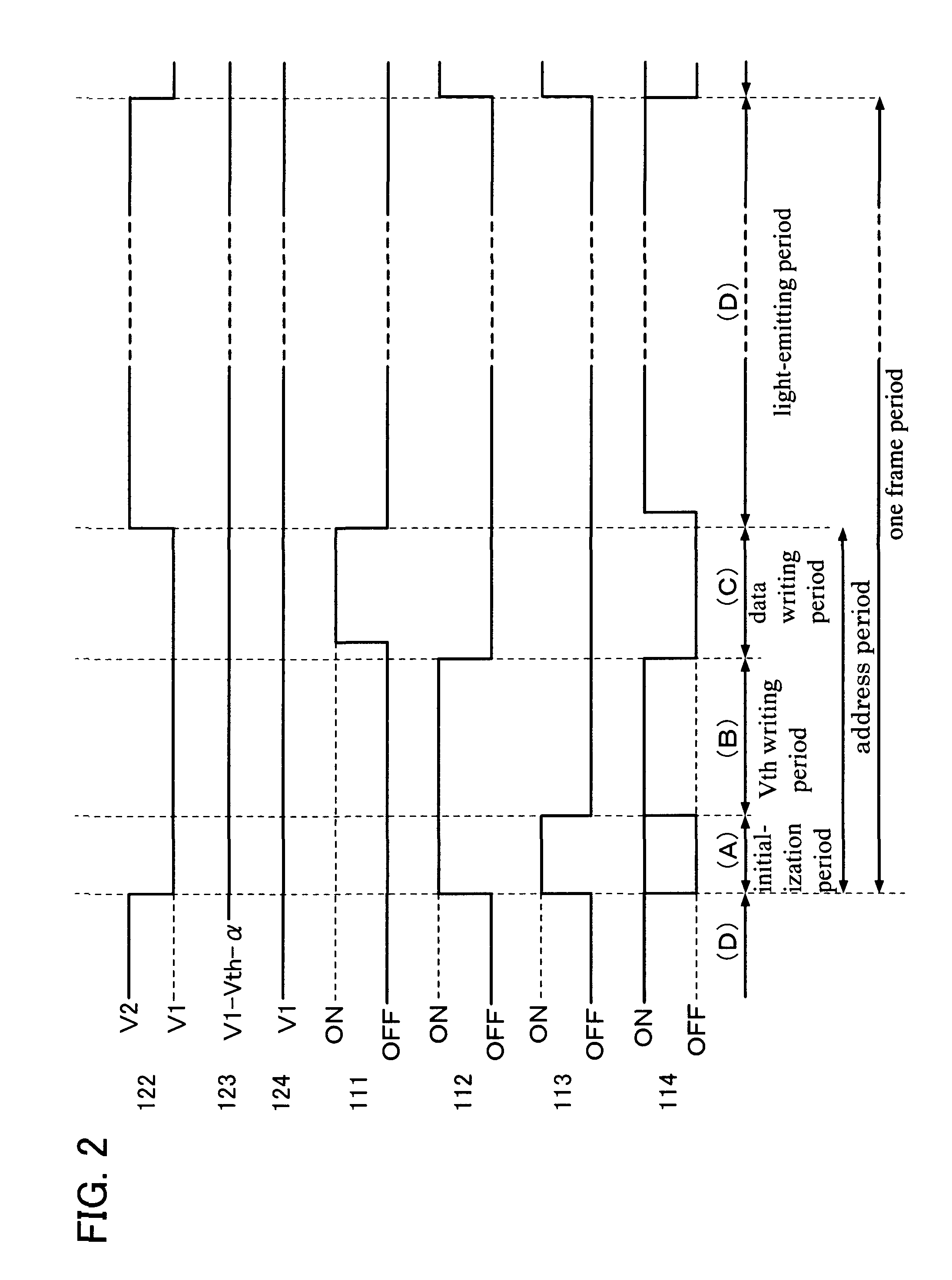
[0104]A basic configuration of a pixel of the invention is described with reference to FIG. 1. A pixel shown in FIG. 1 includes a transistor 110, a first switch 111, a second switch 112, a third switch 113, a fourth switch 114, a capacitor 115, and a light-emitting element 116. Note that the pixel is connected to a signal line 117, a first scan line 118, a second scan line 119, a third scan line 120, a fourth scan line 121, a power supply line 122, and a potential supply line 123. In this embodiment mode, the transistor 110 is an N-channel transistor, and is turned on when a gate-source voltage (Vgs) thereof exceeds the threshold voltage (Vth). In addition, an example is described in which an EL element in which a current is supplied from a pixel electrode 4811 to an opposite electrode 124 is used as the light-emitting element 116 as shown in FIG. 48. In that case, the pixel electrode 4811 of the light-emitting element 116 functions as an anode and the opposite electrode 124 thereof...

embodiment mode 2

[0168]In this embodiment mode, FIG. 11A shows a configuration of a pixel which is different from Embodiment Mode 1. Note that common reference numerals are used for portions which are similar to Embodiment Mode 1 and detailed description of the same portions or portions having similar functions is omitted.

[0169]A pixel shown in FIG. 11A includes the transistor 110, the first switch 111, the second switch 112, the fourth switch 114, a rectifying element 1113, the capacitor 115, and the light-emitting element 116. Note that the pixel is connected to the signal line 117, the first scan line 118, the second scan line 119, a third scan line 1120, the fourth scan line 121, and the power supply line 122. The pixel shown in FIG. 11A has a configuration in which the rectifying element 1113 is used as the third switch 113 in FIG. 3, and the second electrode of the capacitor 115, the first electrode of the transistor 110, and the pixel electrode of the light-emitting element 116 are connected ...

embodiment mode 3

[0175]In this embodiment mode, FIGS. 12 to 15 show configurations each a pixel which is different from Embodiment Modes 1 and 2. Note that although description is made by paying attention to one pixel in Embodiment Modes 1 and 2, the number of wirings can be reduced by sharing a wiring connected to each pixel among pixels. In this case, if normal operation can be performed, various wirings can be shared among the pixels. For example, a wiring can be shared with the next pixel and this embodiment mode shows one example of the method. Note that common reference numerals are used for portions which are similar to Embodiment Mode 1 and detailed description of the same portions or portions having similar functions is omitted.

[0176]A pixel 1200 shown in FIG. 12 includes the transistor 110, the first switch 111, the second switch 112, the third switch 113, the fourth switch 114, the capacitor 115, and the light-emitting element 116. Note that the pixel 1200 is connected to the signal line ...


PUM


Abstract

A pixel includes a load, a transistor which controls a current supplied to the load, a storage capacitor, and first to fourth switches. By inputting a potential in accordance with a video signal into the pixel after the threshold voltage of the transistor is held in the storage capacitor, and holding a voltage of the sum of the threshold voltage and the potential, variations of a current value caused by variations of threshold voltage of a transistor can be suppressed. Consequently, a predetermined current can be supplied to the load such as a light-emitting element. Further, by changing the potential of a power supply line, a display device with a high duty ratio can be provided.

Description

BACKGROUND OF THE INVENTION[0001]1. Field of the Invention[0002]The present invention relates to a semiconductor device having a function for controlling a current supplied to a load with a transistor, and relates to a display device including a pixel which is formed of a current-drive display element, luminance of which is changed in accordance with a signal, and a signal line driver circuit or scan line driver circuit which drives the pixel. In addition, the invention relates to a driving method of such a semiconductor device and a display device. Further, the invention relates to an electronic device having the display device in a display portion.[0003]2. Description of the Related Art[0004]In recent years, a self-luminous display device having a pixel formed by using a light-emitting element such as an electroluminescence (EL) element, that is, a so-called light-emitting device has attracted attention. As a light-emitting element which is used for such a self-luminous display de...

Claims


Application Information

Patent Timeline
IPC IPC(8): G09G3/30
CPCG09G3/3233G09G2300/0819G09G2300/0842G09G2300/0861H01L27/1214G09G2320/0233G09G2320/043H01L27/1222G09G2310/0256H01L29/41733H01L27/1225H01L27/124G09G3/30G09G3/32G09G3/20H05B33/12H10K59/131H10K59/1213G09G3/2003G09G3/2074G09G3/3266G09G2300/0809G09G2310/0291G09G2320/0646G09G2320/0666
Inventor KIMURA, HAJIME
Owner SEMICON ENERGY LAB CO LTD
Why Eureka
Try Eureka