Method for mounting protective covers over image capture devices and devices manufactured thereby

a technology for image capture devices and protective covers, which is applied in the field of electronic devices, can solve the problems of time-consuming and labor-intensive to attach protective covers to each image capture device, adversely affecting images captured by the device, and inability to meet the intended use of the camera module, so as to facilitate the use of thin protective covers, improve manufacturing quality and yield, and improve the effect of quality

Inactive Publication Date: 2007-10-11
FLEXTRONICS AP LLC
View PDF50 Cites 18 Cited by
  • Summary
  • Abstract
  • Description
  • Claims
  • Application Information

AI Technical Summary

Benefits of technology

[0011] The present invention overcomes the problems associated with the prior art by providing methods for mounting protective covers over image capture devices of camera modules that are cheaper, faster, and more efficient than known methods. Methods of the invention have higher manufacturing quality and yield, and facilitates the use of thinner protective covers. Methods of the present invention also reduce the time and expense of preparing the protective covers for mounting and protect the image capture devices against contamination early in the assembly process. The described methods, and / or variations thereof, each provide some, but not necessarily all, of the foregoing advantages.

Problems solved by technology

Some known camera modules include a protective glass cover mounted over the sensor array of the image capture device to protect the sensor area from contamination, which will adversely affect images captured by the device and render the camera module unacceptable for its intended use.
Although the protective covers are somewhat effective to prevent contamination of the sensor array, there are some drawbacks to their use.
One disadvantage associated with current methods of mounting protective covers over image capture devices is that it is time consuming to attach the covers to each image capture device.
Another disadvantage of known methods is that the protective glass covers need to be thicker than is often desired.
The reason for the thicker glass is that the automated equipment used to place the glass covers is incapable of handling glass less than about 300 microns thick without breaking it.
As a result, the thicker glass unnecessarily increases the thickness and / or weight of the device.
Another disadvantage is the cost and / or time required to prepare the glass covers.
The machinery used to perform the glass sawing operations is expensive, and the time required is substantial.
Thus, the time and cost of preparing the protective covers is substantial.
Another problem with the methods of the prior art are that the protective covers can only protect the sensor array after they are mounted on the image capture device.
Therefore, the device is susceptible to contamination by foreign particles during any assembly steps that occur prior to mounting the cover.
For example, contamination can result from handling of the image capture devices prior to mounting on the PCB, the process of soldering the image capture devices to the PCB, cleaving of the PCB, or even from the singulation process of separating the image capture devices from the unitary substrate on which they are formed.
To compound the problem of contamination, once the protective cover is applied, any contaminants on the sensor array will be trapped, thereby resulting in a permanently defective image capture device.

Method used


Image

  • Method for mounting protective covers over image capture devices and devices manufactured thereby
  • Method for mounting protective covers over image capture devices and devices manufactured thereby
  • Method for mounting protective covers over image capture devices and devices manufactured thereby

Examples


Embodiment Construction

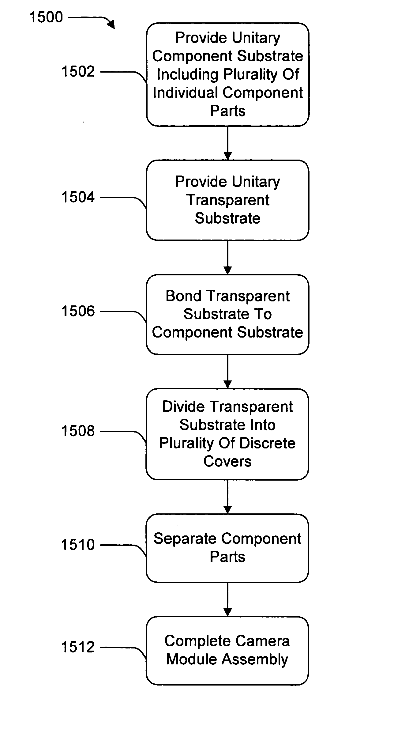
[0042] Particular embodiments of the present invention will now be described with reference to the drawings. In the following description, numerous specific details are set forth (e.g., certain manufacturing and assembly processes, example lens housings, etc.) in order to provide a thorough understanding of the invention. Those skilled in the art will recognize, however, that the invention may be practiced apart from these specific details. In other instances, details of well known manufacturing practices (e.g., semiconductor fabrication, optical bonding, component mounting, etc.) and components have been omitted, so as not to unnecessarily obscure the present invention. It should be understood that the full scope of the invention is not limited by this detailed description of particular embodiments of the invention.

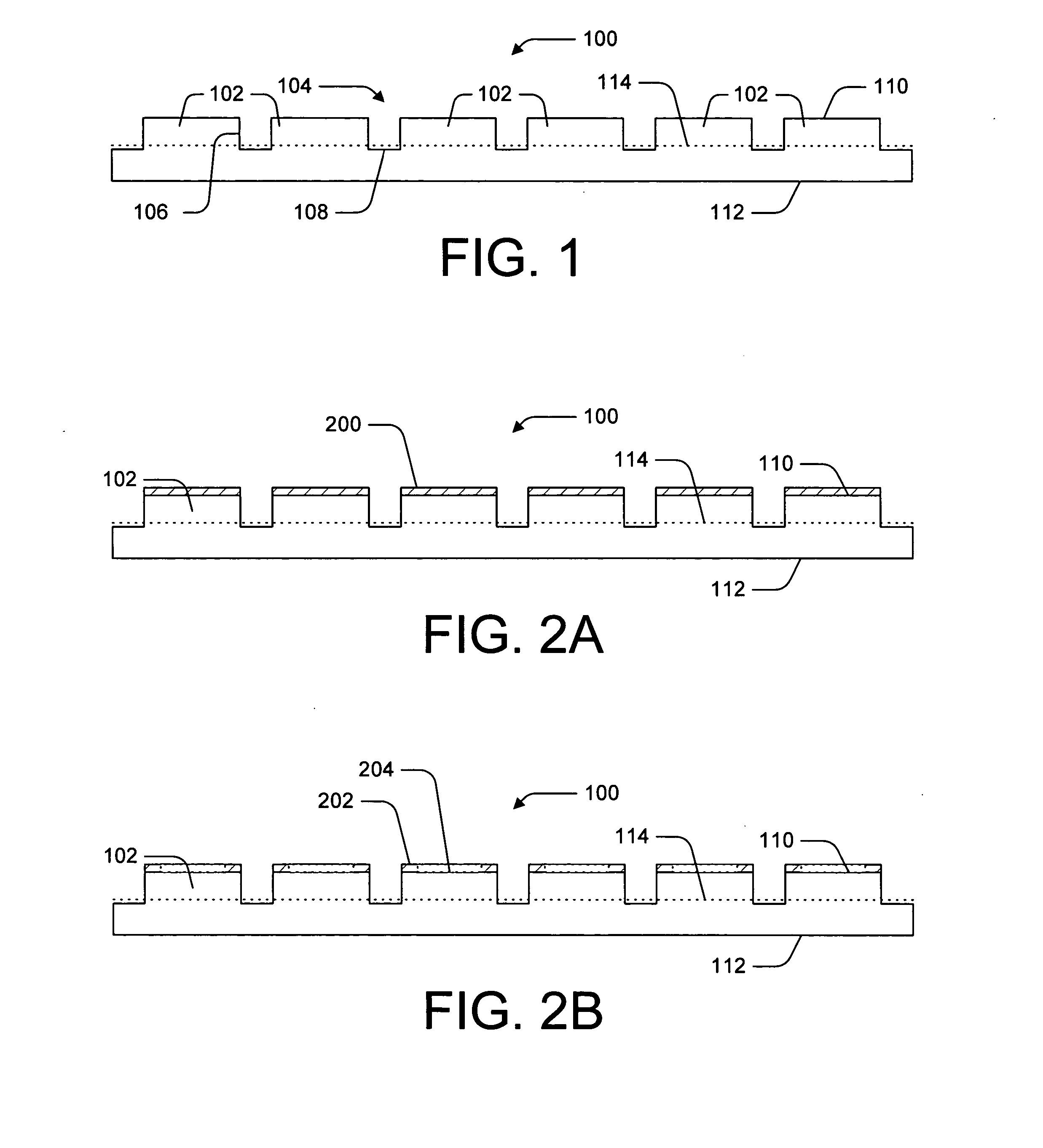
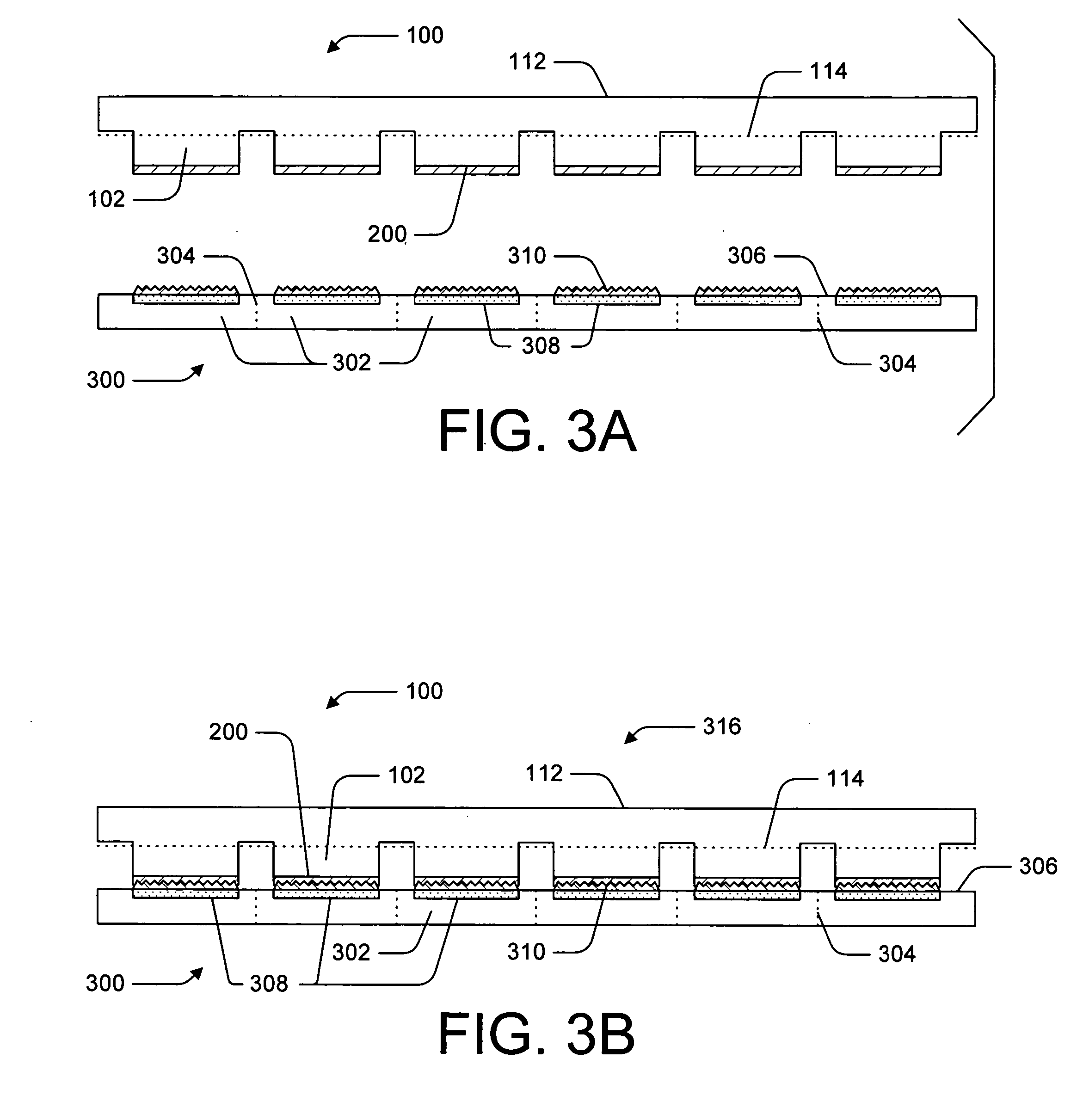
[0043]FIG. 1 is a cross-sectional view of a unitary transparent substrate 100 that includes a plurality of individual protective covers 102 partially defined by a plura...


PUM

PropertyMeasurementUnit
thicknessaaaaaaaaaa
thickaaaaaaaaaa
thickaaaaaaaaaa

Abstract

A method for manufacturing camera modules including image capture devices with protective covers is disclosed. The method includes providing a unitary transparent substrate including a plurality of individual protective covers, providing a unitary component substrate including a plurality of individual component parts, bonding the unitary transparent substrate to the unitary component substrate, dividing the transparent substrate into a plurality of discrete protective covers, and separating the component parts from one another. According to one particular method, the component substrate is a semiconductor wafer having a plurality of integrated electronic image capture devices formed therein. According to another particular method, the component substrate is a circuit board having a plurality of individual device circuit boards formed therein.

Description

BACKGROUND OF THE INVENTION [0001] 1. Field of the Invention [0002] This invention relates generally to electronic devices, and more particularly to digital camera modules. More particularly, this invention relates to a method for manufacturing digital camera modules including image capture devices with protective covers mounted thereon. [0003] 2. Description of the Background Art [0004] Electronic camera modules are currently included in various consumer electronic products such as mobile telephones and hand-held electronic organizers. These camera modules typically include a CCD or CMOS image sensor and a lens assembly mounted on a printed circuit board (PCB). The camera module is then mounted on a PCB of the host device. [0005] Some known camera modules include a protective glass cover mounted over the sensor array of the image capture device to protect the sensor area from contamination, which will adversely affect images captured by the device and render the camera module unacc...

Claims


Application Information

Patent Timeline
Patent Type & Authority Applications(United States)
IPC IPC(8): H04N5/335H01S4/00
CPCH01L27/14618H01L27/1462H01L27/14625H01L27/14683Y10T29/49002H04N5/2257H04N5/2254Y10T29/4913H01L27/14685H01L2924/0002H04N23/57H04N23/631H01L2924/00
Inventor TAM, SAMUEL WAISINGSHANGGUAN, DONGKAI
Owner FLEXTRONICS AP LLC
Why Eureka
Try Eureka