
Method for forming polycrystalline film

a polycrystalline film and film technology, applied in the field of polycrystalline film forming, can solve the problems of deterioration of productivity, reducing reliability and yield, and a-si tft not meeting the operation velocity required in the driving elements of the peripheral circuit, so as to prevent the deterioration of productivity

Inactive Publication Date: 2007-10-11
BOE HYDIS TECH
View PDF5 Cites 4 Cited by
  • Summary
  • Abstract
  • Description
  • Claims
  • Application Information

AI Technical Summary

Benefits of technology

[0017]Accordingly, the present invention has been developed in order to solve the above-mentioned problems occurring in the prior art, and an object of the present invention is to provide a method for forming polycrystalline film, which can prevent the deterioration of the productivity which is caused by the laser beam irradiated several times.
[0018]Another object of the present invention is to provide a method for forming polycrystalline film, which can prevent the deterioration of the characteristics and the uniformity of poly-Si TFT which is caused by an uneven size of crystal grains and uneven forming of high angle grain boundary.
[0024]The transparent region has a size enough to prevent creation of nucleation.

Problems solved by technology

Meanwhile, since an a-Si TFT in which the a-Si is used as the active layer has a significantly low mobility of about 0.5 cm2 / Vs, it is restrictive that all switching elements used for the liquid crystal displays are made of the a-Si TFT.
Specifically, although driving elements for peripheral circuits of the liquid crystal displays are operated at a rapid velocity, the a-Si TFT cannot satisfy operation velocity required in the driving elements for the peripheral circuits.
Therefore, this means that it becomes eventually difficult to realize the driving elements for the peripheral circuits using the a-Si TFT.
In this case, the glass substrate is deformed at temperatures higher than 600° C., thereby causing a reduction in reliability and yield.
Thus, this causes the deterioration of productivity.
Further, as the poly-Si has a size of crystal grain which is different between the portion in which the laser beam overlaps and the portion in which the laser beam does not overlap, there exists a problem in that the characteristics of the poly-Si TFT is deteriorated.
However, controlling of the position of the high angle grain boundary is difficult, so that the characteristics of the poly-Si TFT become deteriorated.

Method used


Image

  • Method for forming polycrystalline film
  • Method for forming polycrystalline film
  • Method for forming polycrystalline film

Examples


Embodiment Construction

[0036]Hereinafter, the preferred embodiment of the present invention will be described with reference to the accompanying drawings.

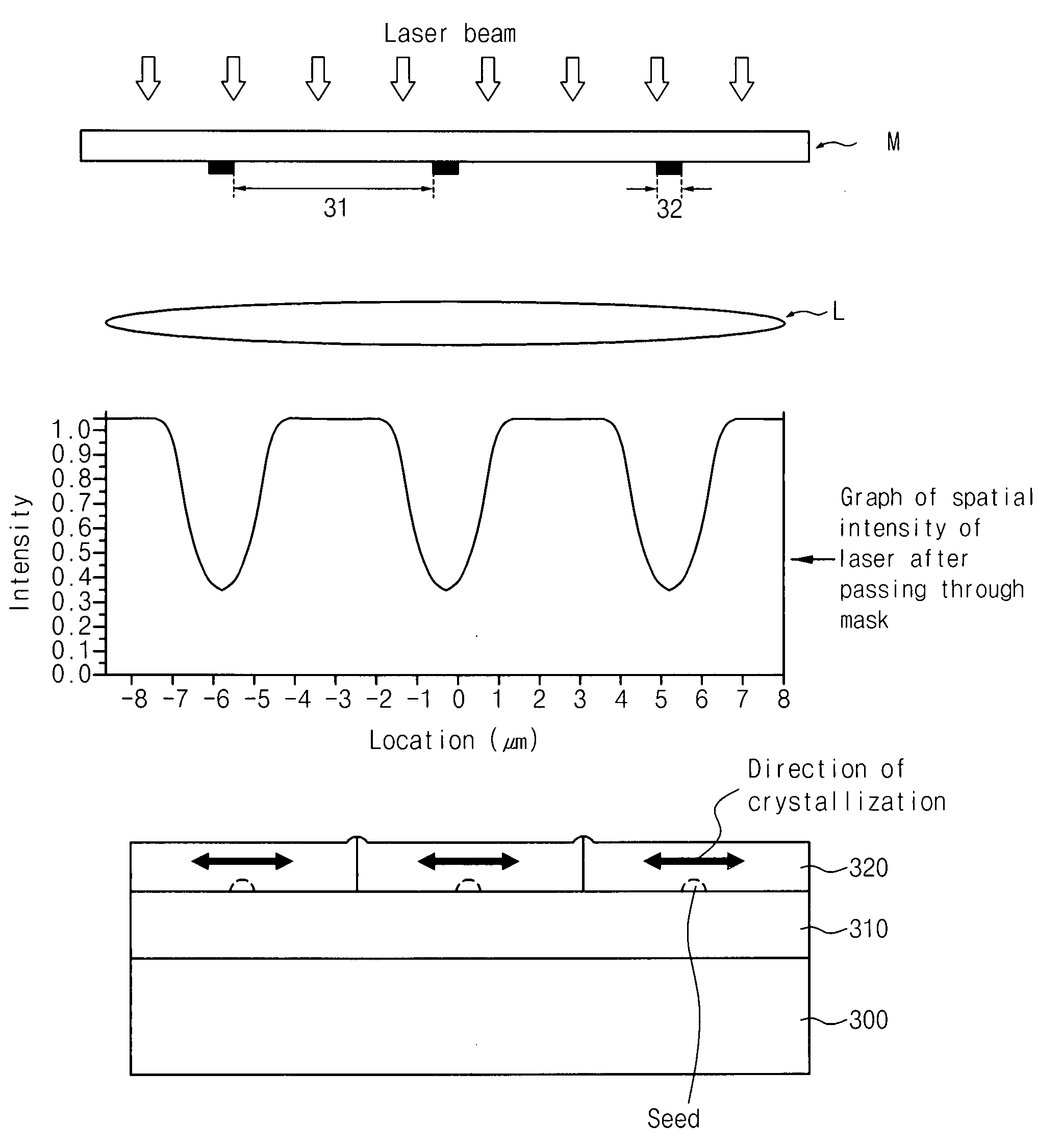
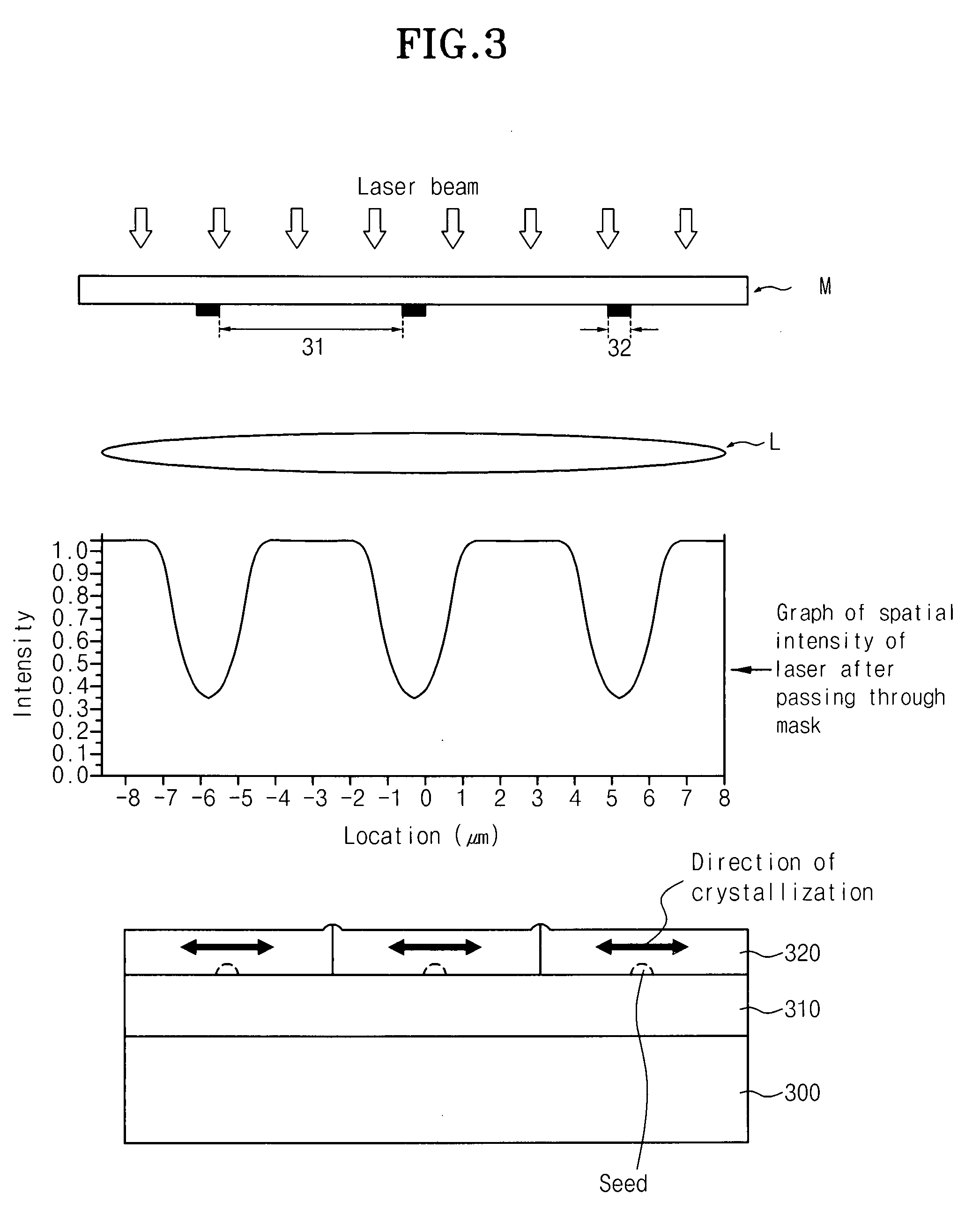
[0037]First, the technical principle of the present invention will be described in brief. The present invention presents a method for forming a poly-Si film, in which a laser beam is irradiated to a-Si film, which is deposited on a glass substrate in a state that a buffer layer is interposed between the a-Si film and the glass substrate, by using a mask, so as to crystallize the a-Si film. At this time, the laser beam is irradiated at maximum intensity to a portion of the a-Si film under a transparent region of the mask while being irradiated at minimum intensity exceeding zero to another portion of the a-Si film under an opaque region of the mask, by using the mask including a larger transparent region than a limitation size of the resolution of a laser beam equipment and a smaller opaque region than a limitation size of the resolution of the laser beam...


PUM

PropertyMeasurementUnit
Sizeaaaaaaaaaa
Transparencyaaaaaaaaaa
Distanceaaaaaaaaaa

Abstract

Disclosed is a method for forming a polycrystalline film. The method for forming a polycrystalline film from a film deposited on a glass substrate while a buffer layer is interposed between the deposited film and the glass substrate, which includes the steps of: preparing a mask including a transparent region having a larger size than that of resolution limitation of a laser beam equipment and an opaque region having a size which is smaller than that of the resolution limitation of the laser beam equipment; and irradiating laser beam of the maximum intensity to a film under the transparent region while irradiating the laser beam having a minimum intensity exceeding zero to the film under an opaque region by using the mask, thereby crystallizing the film by single irradiation of the laser beam.

Description

BACKGROUND OF THE INVENTION[0001]1. Field of the invention[0002]The present invention relates to a method for forming a polycrystalline film, and more particularly to a method for forming polycrystalline silicon film in order to form polycrystalline silicon transistors.[0003]2. Description of the Prior Art[0004]Thin Film Transistors (hereinafter, referred to as TFT), which are used as switching elements in liquid crystal displays or organic Electro Luminescence displays, are very important structural elements in an aspect of performance of flat panel display. Herein, mobility or leakage current, etc., which is used as a reference for determining the performance of TFT, is greatly influenced by a status or a structure of active layer which is a pathway through which charge carriers move, i.e. by a status or a structure of silicon thin film which is material for the active layer. Currently, in the case of commercially available liquid crystal display, the active layer of the TFT is mo...

Claims


Application Information

Patent Timeline
IPC IPC(8): H01L21/20
CPCB23K26/0656H01L21/02422H01L21/02532H01L21/0254H01L27/1296H01L21/0268H01L21/02686H01L21/02691H01L27/1285H01L21/02546B23K26/066
Inventor KIM, EOK SURYU, MYUNG KWANSON, GONKWON, HYUK SOONPARK, JUNG HO
Owner BOE HYDIS TECH
Learn More