Thin film transistor

a transistor and film technology, applied in the field of thin film transistors, can solve the problems of increasing the drain current and the saturation current affecting the quality of analog circuit characteristics, and achieve the effect of reducing the channel length modulation effect and reducing the kink

Inactive Publication Date: 2007-10-18
MITSUBISHI ELECTRIC CORP
View PDF10 Cites 17 Cited by
  • Summary
  • Abstract
  • Description
  • Claims
  • Application Information

AI Technical Summary

Benefits of technology

[0005]An object of the present invention is to provide a thin film transistor capable of reducing the kink effect as well as reducing the channel length modulation effect.

Problems solved by technology

In thin film transistors, high electric fields may be formed near the drain, resulting in impact ionization, which increases the drain current.
The kink effect is indeed suppressed by splitting a gate electrode into a plurality of portions and providing a silicon layer between the split portions of the gate electrode as described in the above gazette; however, the saturation current which affects the quality of analog circuit characteristics is still large.

Method used


Image

  • Thin film transistor
  • Thin film transistor
  • Thin film transistor

Examples


first preferred embodiment

[0025]The present embodiment will describe a thin film transistor including first and second transistors with first and second gate electrodes provided separately from each other on the surface of a gate insulating film. The thin film transistor is intended to reduce an electric field concentration at the channel edge on the drain side by setting the threshold voltage of the second transistor lower than that of the first transistor.

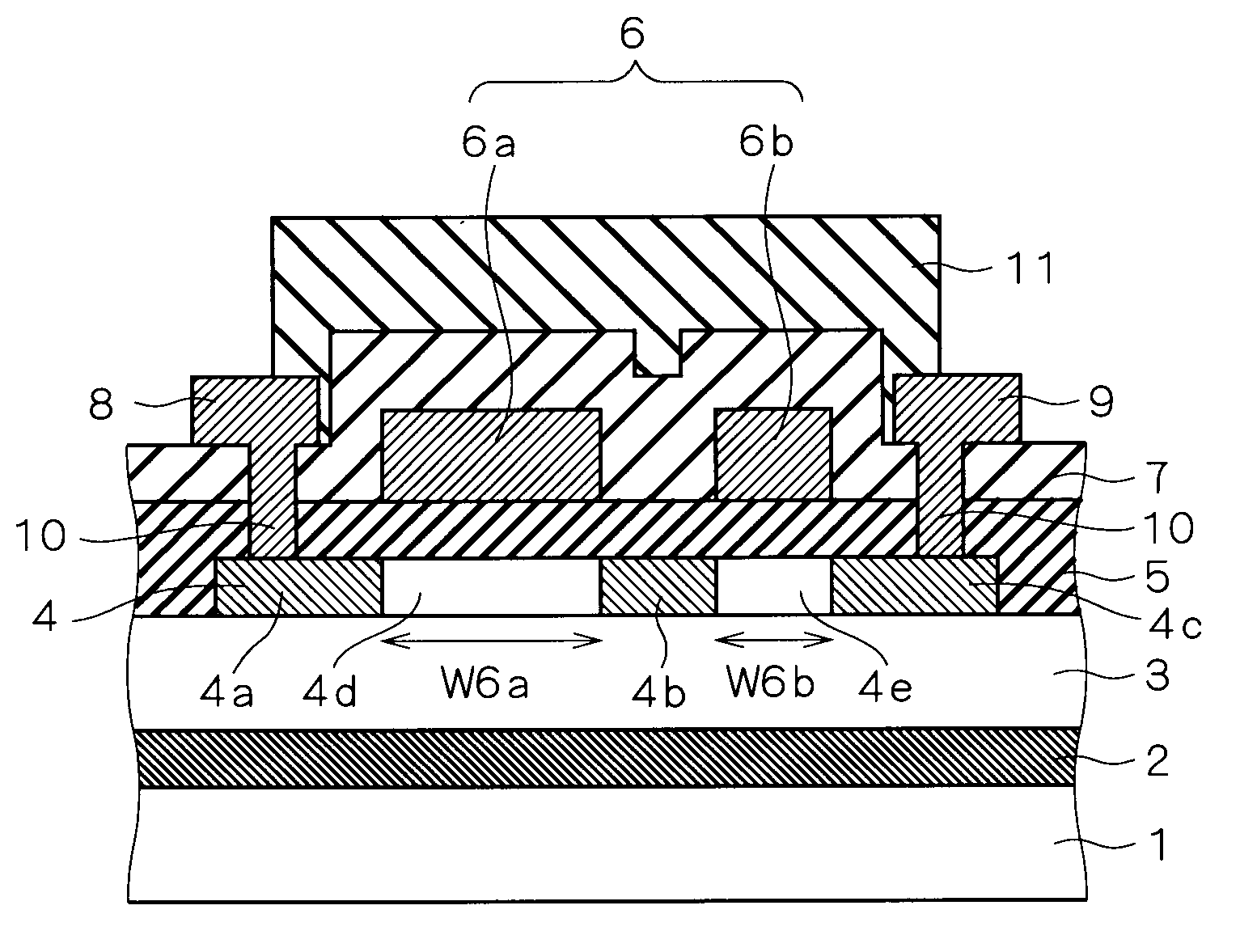
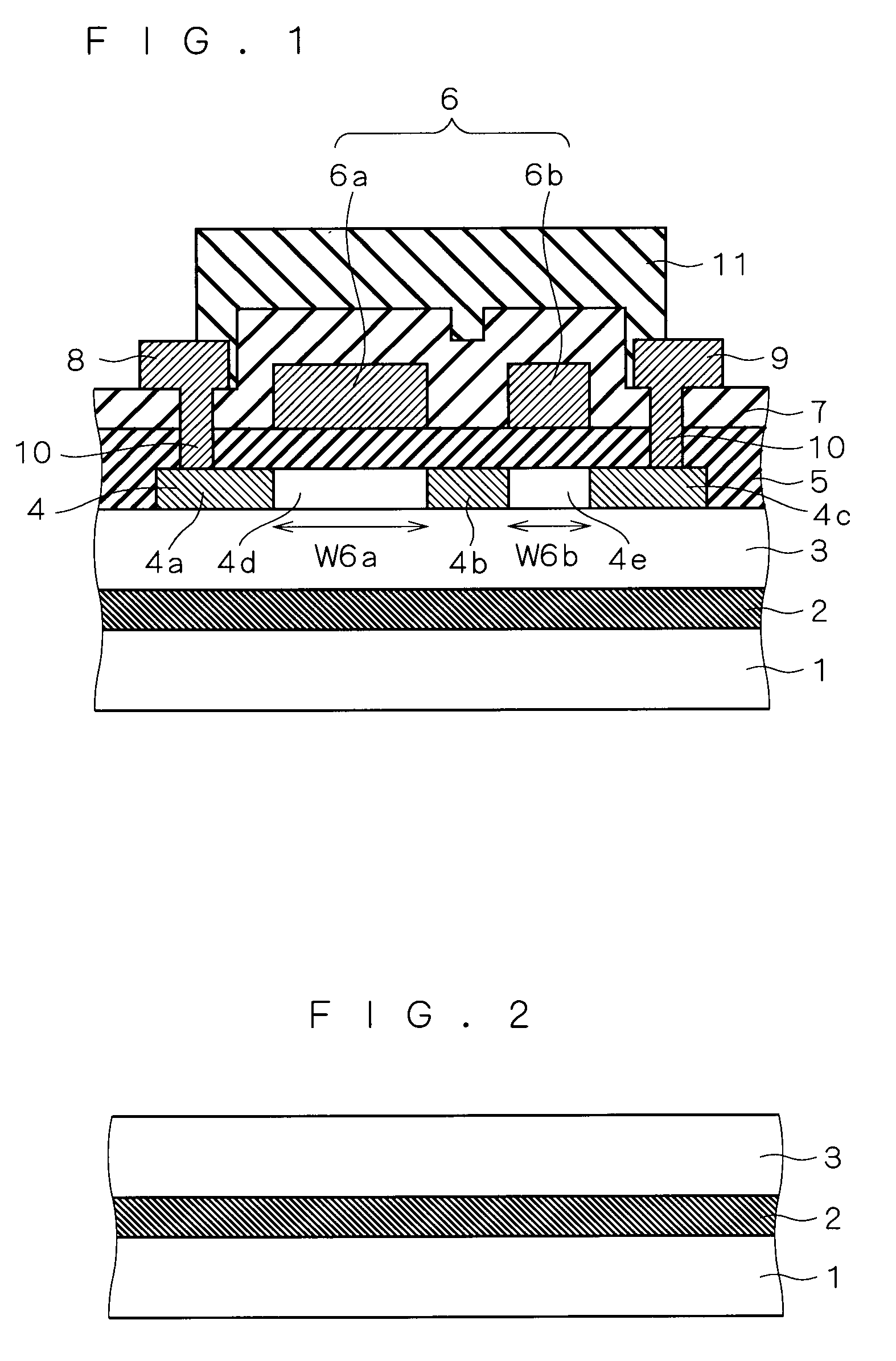
[0026]FIG. 1 is a sectional view showing the thin film transistor according to the present embodiment. The thin film transistor includes a glass substrate 1. A 100-nm thick silicon nitride (SiN) film 2 and a 200-nm thick silicon oxide (SiO2) film 3 are formed on the glass substrate 1.

[0027]A polycrystalline silicon (polysilicon) film 4 is formed like islands on the silicon oxide film 3. That is, the polysilicon film 4 is a semiconductor layer formed above the glass substrate 1. Formed on the surfaces of the polysilicon film 4 and silicon oxide film 3 is a...

second preferred embodiment

[0058]The present embodiment is a modification of the thin film transistor according to the first preferred embodiment, in which the threshold voltage of the second transistor is set lower than that of the first transistor by making the first and second transistors differ in impurity concentration at the channel.

[0059]FIG. 10 is a sectional view showing a thin film transistor according to the present embodiment. The thin film transistor includes a glass substrate 101. A 100-nm thick silicon nitride (SiN) film 102 and a 200-nm thick silicon oxide film 103 are formed on the glass substrate 101.

[0060]A polysilicon film 104 is formed like islands on the silicon oxide film 103. That is, the polysilicon film 104 is a semiconductor layer formed above the glass substrate 101. Formed on the surfaces of the polysilicon film 104 and silicon oxide film 103 is a silicon oxide film 105 serving as a gate insulating film.

[0061]A first gate electrode 106a and a second gate electrode 106b, each being...

third preferred embodiment

[0085]The present embodiment is another modification of the thin film transistor according to the first preferred embodiment, in which the threshold voltage of the second transistor is set lower than that of the first transistor by making the first and second transistors differ in crystal defect density at the channel.

[0086]FIG. 20 is a sectional view showing a thin film transistor according to the present embodiment. The thin film transistor includes a glass substrate 201. A 100-nm thick silicon nitride film 202 and a 200-nm thick silicon oxide film 203 are formed on the glass substrate 201.

[0087]A polysilicon film 204 is formed like islands on the silicon oxide film 203. That is, the polysilicon film 204 is a semiconductor layer formed above the glass substrate 201. Formed on the surfaces of the polysilicon film 204 and silicon oxide film 203 is a silicon oxide film 205 serving as a gate insulating film.

[0088]A first gate electrode 206a and a second gate electrode 206b, each being...


PUM


Abstract

In first and second gate electrodes constituting a gate electrode, the gate length of the second gate electrode is set shorter than the gate length of the first gate electrode and short enough to produce the short channel effect. The threshold voltage of a second transistor corresponding to the second gate electrode can thereby be made lower than the threshold voltage of a first transistor corresponding to the first gate electrode. When the same voltage is applied to the first and second gate electrodes, an electric field concentration at the channel edge on the drain side is reduced. This in result reduces the channel length modulation effect.

Description

FIELD OF THE INVENTION[0001]The present invention relates to a thin film transistor for use in an analog circuit for a liquid crystal display or an organic EL display.DESCRIPTION OF THE BACKGROUND ART[0002]In thin film transistors, high electric fields may be formed near the drain, resulting in impact ionization, which increases the drain current. This phenomenon is called the kink effect. National Publication of Translation No. 2003-519917 (WO01 / 050514) describes a technique of reducing such kink effect.[0003]The above gazette discloses the technique of splitting the gate electrode into a plurality of portions so that carriers are absorbed into a silicon layer between the split portions of the gate electrode, to thereby suppress the kink effect.[0004]The kink effect is indeed suppressed by splitting a gate electrode into a plurality of portions and providing a silicon layer between the split portions of the gate electrode as described in the above gazette; however, the saturation c...

Claims


Application Information

Patent Timeline
Patent Type & Authority Applications(United States)
IPC IPC(8): H01L29/04
CPCH01L29/78645H01L27/1214H01L29/78618H01L29/78696
Inventor TOKIOKA, HIDETADANAKAGAWA, NAOKIAGARI, MASAFUMI
Owner MITSUBISHI ELECTRIC CORP
Why Eureka
Try Eureka