This helps you quickly interpret patents by identifying the three key elements:
Problems solved by technology
Method used
Benefits of technology
Benefits of technology
[0021]The present invention is made to solve the aforementioned problems. An object of the present invention is to provide a nonvolatile semiconductor memory device which can prevent a parasitic bipolar operation and is suitable for higher integration.
[0025]Moreover, since the control gate impurity diffusion region is isolated and insulated from other element formation regions by the isolation insulating layer, unlike the conventional example, the diffusion length of an impurity does not have to be considered in isolating elements from each other. Therefore, the two-dimensional occupation area of a memory cell can be reduced compared with the conventional example, so that a memory cell suitable for higher integration can be obtained.
Problems solved by technology
However, the latter application has been present for a long time and has been demanded in particular for Mixed Signal IC (Integrated Circuit).
Therefore, the memory cell is fabricated through complicated processes and therefore is not suitable for the small capacity application.
However, the conventional 1poly-type nonvolatile semiconductor memory device has the following problems.
However, when a negative voltage is applied to this n-type impurity diffusion region, the p-type region of the semiconductor substrate and the n-type impurity diffusion region as a control gate are biased in the forward direction so that a large current flows thereby disabling the operation.
Accordingly, the p-type impurity diffusion region as a control gate, the n-type impurity diffusion region and the p-type region of the semiconductor substrate operate as parasitic bipolar, causing an operating error.
Therefore, this memory cell is not suitable for higher integration.
Method used
Image
Click on the blue label to locate the original text in one second.
Reading with bidirectional positioning of images and text.
Examples
first embodiment
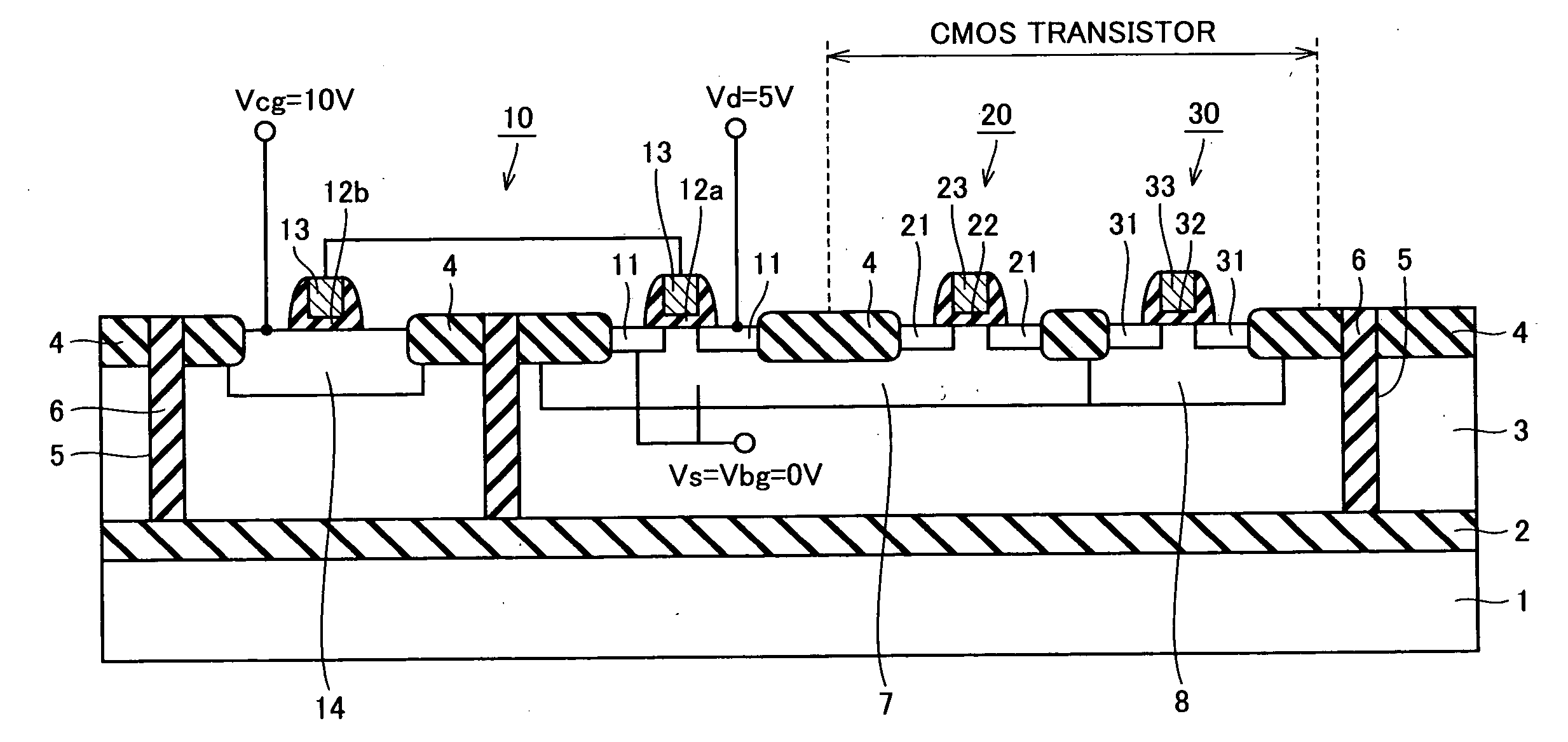
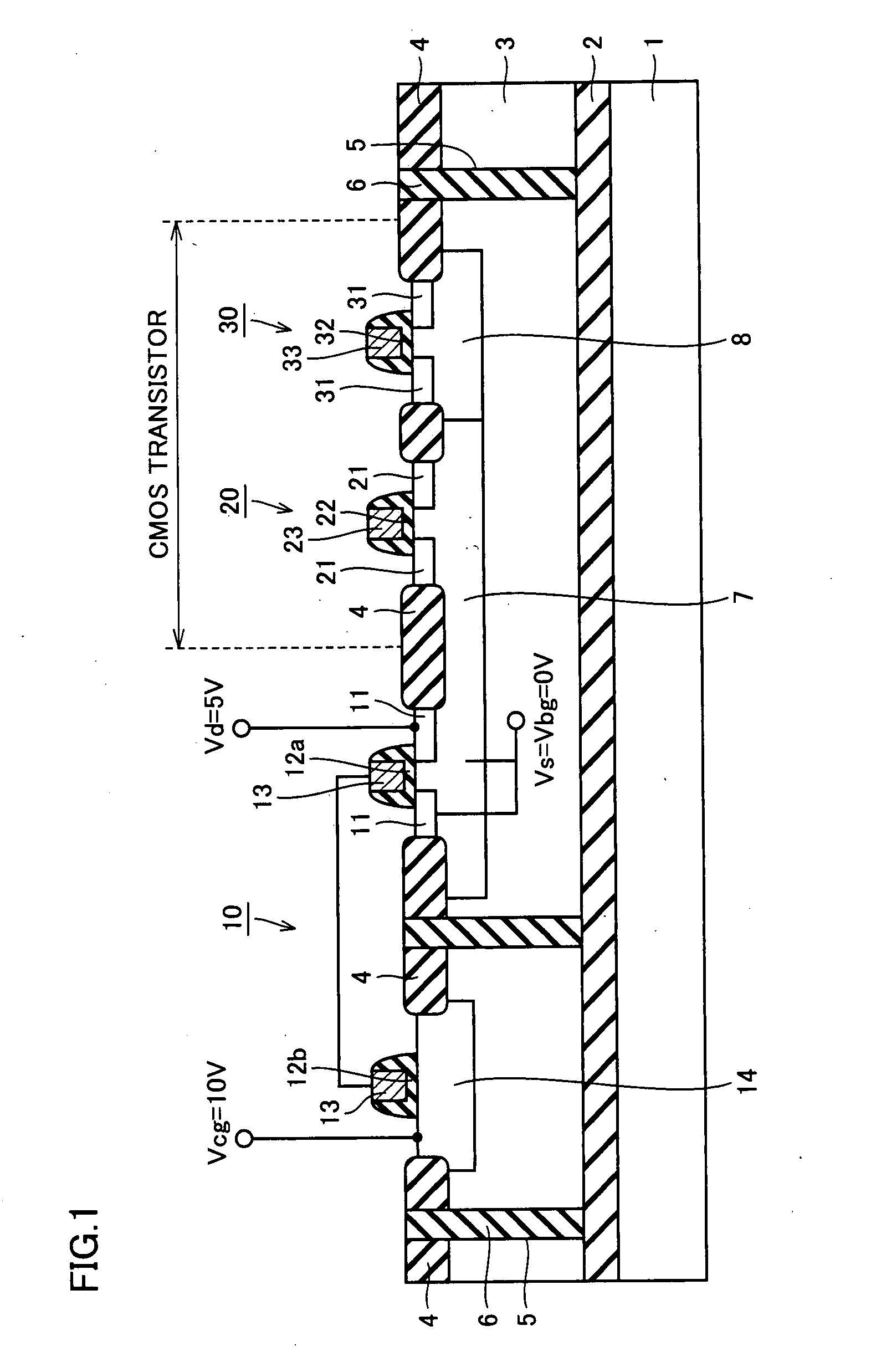
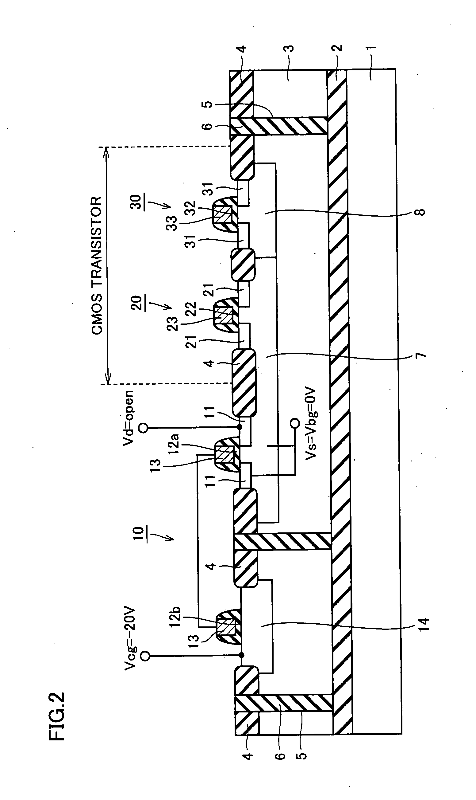
[0047]Referring to FIG. 1, in the present embodiment, a 1poly-type memory cell 10 is formed at SOI (Silicon on Insulator) substrate 1, 2, 3.
[0048]The SOI substrate has a support substrate 1, a buried insulating layer 2 formed, for example, of a siliconoxide film on support substrate 1, and an n− or p− semiconductor layer 3 formed, for example, of silicon on buried insulating layer 2. A field insulating layer 4 formed, for example, of a siliconoxide film is formed at a part of the surface of semiconductor layer 3. Here, buried insulating layer 2 is for example a BOX (Buried Oxide) layer.
[0049]The 1poly-type memory cell 10 mainly has a pair of n-type source / drain regions 11, 11, a floating gate electrode layer 13, and a control gate impurity diffusion region 14. A pair of source / drain regions 11, 11 is formed at a surface of a p-type well 7 formed at the surface of semiconductor layer 3. Floating gate electrode layer 13 is formed, for example, of polysilicon doped with an impurity a...
second embodiment
[0077]Referring to FIG. 15, in this embodiment, groove 5 is formed in semiconductor layer 3 to surround the periphery of source / drain region 11 and back gate layer (p-type well) 7 of the 1poly-type memory cell 10. Isolation insulating layer 6, for example, formed of a silicon oxide film is filled in this groove 5. Accordingly, isolation insulating layer 6 extends from the surface of semiconductor layer 3 to reach buried insulating layer 2 while surrounding the periphery of source / drain region 11 and back gate (p-type well) 7 and separates source / drain region 11 and back gate (p-type well) 7 from other element formation regions (for example, the formation region of CMOS transistors 20, 30).
[0078]Isolation insulating layer 6 surrounding the periphery of source / drain region 11 and back gate (p-type well) 7 and isolation insulating layer 6 surrounding the periphery of control gate impurity diffusion region 14 partially share an insulating layer portion.
[0088]Referring to FIG. 17, the configuration of the present embodiment differs from the configuration of the first embodiment in that an isolation region 3a formed of a semiconductor layer is provided between isolation insulating layer 6 surrounding the periphery of control gate impurity diffusion region 14 and isolation insulating layer 6 surrounding the periphery of source / drain region 11 and CMOS transistors 20, 30.
[0089]It is noted that the other configuration is almost the same as the configuration of the first embodiment. Therefore the same elements will be denoted with the same reference characters and a description thereof will not be repeated.
PUM
Abstract
An SOI substrate is comprised of a support substrate, a buried insulating layer and a semiconductor layer. A 1poly-type memory cell has a pair of source / drain regions, a floating gate electrode layer, and a control gate impuritydiffusion region. An isolation insulating layer extends from a surface of the semiconductor layer to reach the buried insulating layer while surrounding the periphery of the control gate impuritydiffusion region thereby to separate a region in which the source / drain regions are formed and the control gate impuritydiffusion region from each other. Therefore, a nonvolatile semiconductor can be obtained which can prevent a parasitic bipolar operation and is suitable for higher integration.
Description
BACKGROUND OF THE INVENTION[0001]1. Field of the Invention[0002]The present invention relates to a nonvolatile semiconductor memory device.[0003]2. Description of the Background Art[0004]Applications of nonvolatile semiconductor memory devices are divided into the relatively mass storage application and the small capacity application. The former is the application of data storage for music or images or code storage, with a capacity of a few hundreds of kbits. The latter is the application of (1) storage of address data of LAN (local Area Network) or the like or encryption data for security and (2) trimming of a resistance element, with the capacity of at most a few kbits.[0005]In general, a nonvolatile semiconductor memory device refers to the former, which is technically mainstream. However, the latter application has been present for a long time and has been demanded in particular for Mixed Signal IC (Integrated Circuit).[0006]However, the mass-storage nonvolatile semiconductor me...
Claims
Application Information
Patent Timeline
Application Date:The date an application was filed.
Publication Date:The date a patent or application was officially published.
First Publication Date:The earliest publication date of a patent with the same application number.
Issue Date:Publication date of the patent grant document.
PCT Entry Date:The Entry date of PCT National Phase.
Estimated Expiry Date:The statutory expiry date of a patent right according to the Patent Law, and it is the longest term of protection that the patent right can achieve without the termination of the patent right due to other reasons(Term extension factor has been taken into account ).
Invalid Date:Actual expiry date is based on effective date or publication date of legal transaction data of invalid patent.

