Method of forming a phase change material layer, method of forming a phase change memory device using the same, and a phase change memory device so formed

a memory device and phase change technology, applied in the direction of solid-state devices, coatings, chemical vapor deposition coatings, etc., can solve the problems of difficult high-integration large power consumption of phase-change memory devices, and significant amount of current required to generate this much heat. high-integration and low power consumption

Active Publication Date: 2007-10-25
SAMSUNG ELECTRONICS CO LTD
View PDF8 Cites 55 Cited by
  • Summary
  • Abstract
  • Description
  • Claims
  • Application Information

AI Technical Summary

Benefits of technology

[0011]It is therefore a feature of an embodiment of the present invention to provide a method of forming a phase change material layer that may selectively form the phase change material layer on a conductive feature.
[0012]It is therefore another feature of an embodiment of the present invention to provide a method of forming a phase change material layer that may form the phase change material layer on the conductive feature without forming the phase change material on an adjacent insulator, which may eliminate the formation of overhangs, seams and / or voids in the phase change material layer.
[0013]It is therefore a further feature of an embodiment of the present invention to provide a phase change memory device having a phase change material layer that is uniformly formed and has a small contact area, such that the phase change memory device may be used for a highly integrated, low power consumption memory.
[0014]At least one of the above and other features and advantages of the present invention may be realized by providing a method of forming a phase change material layer, including preparing a substrate having an insulator and a conductor, loading the substrate into a process housing, injecting a deposition gas into the process housing to selectively form a phase change material layer on an exposed surface of the conductor, and unloading the substrate from the process housing, wherein a lifetime of the deposition gas in the process housing is shorter than a time the deposition gas takes to react by thermal energy.

Problems solved by technology

A significant amount of current may be required to generate this much heat.
Accordingly, the phase change memory device may exhibit a large power consumption.
In addition, it may be difficult to highly integrate the phase change memory device, because a channel width of a MOS transistor in the phase change memory device may need to be increased in order to control the high current.
Voids and seams may degrade the operational characteristics of the phase change material layer.
For example, a portion of the phase change material layer where the void or seam is formed may have a very high resistance, which may make detecting changes in resistance due to transformations between the crystalline and amorphous states difficult or impossible to sense accurately.
In addition, voids and seams may reduce the uniformity of unit cells in a phase change memory device, such that programming resistances, erasing resistances, the amount of program and erase current, etc., may be non-uniform, degrading the operation of the phase change memory device.

Method used


Image

  • Method of forming a phase change material layer, method of forming a phase change memory device using the same, and a phase change memory device so formed
  • Method of forming a phase change material layer, method of forming a phase change memory device using the same, and a phase change memory device so formed
  • Method of forming a phase change material layer, method of forming a phase change memory device using the same, and a phase change memory device so formed

Examples


first embodiment

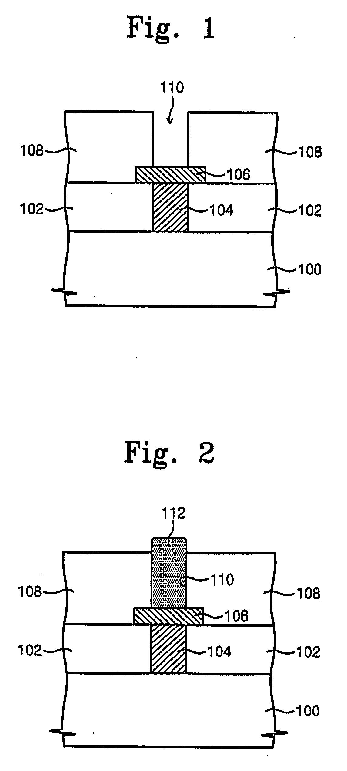
[0037]FIGS. 1 through 3 illustrate cross-sectional views of stages in a method of forming a phase change memory device according to the present invention. Referring to FIG. 1, a lower insulating layer 102 may be formed on a substrate 100, which may be, e.g., a semiconductor substrate. The lower insulating layer 102 may be formed of, e.g., an oxide layer. A lower plug 104 may be formed through the lower insulating layer 102. The lower plug 104 may be in contact with the substrate 100. The lower plug 104 may be formed of, e.g., a conductive material such as doped polysilicon, a metal such as tungsten, a conductive metal nitride such as titanium nitride or tantalum nitride, a metal silicide such as tungsten silicide or titanium silicide, etc.

[0038]A switching device may be formed on the substrate 100 to be in contact with the lower plug 104. For example, one end of a PN diode may be formed on the substrate 100 to be in contact with the lower plug 104. In another implementation, source / ...

third embodiment

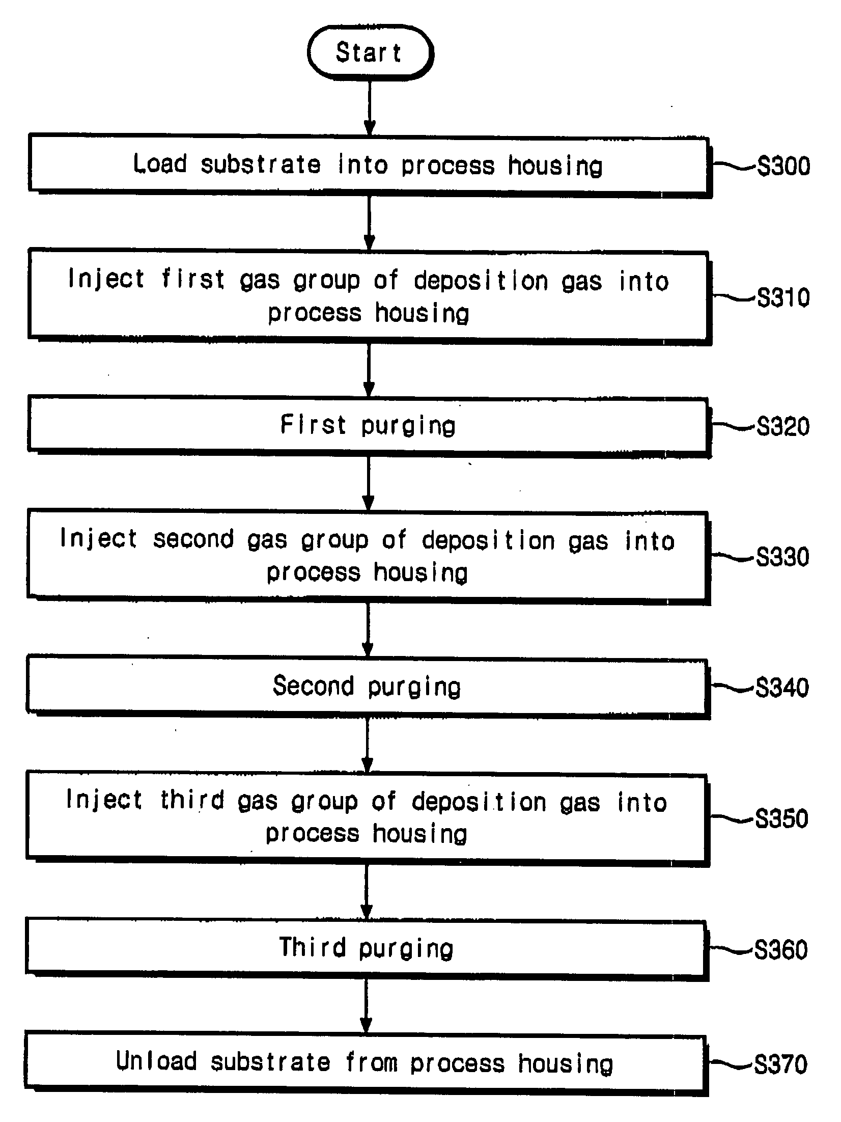
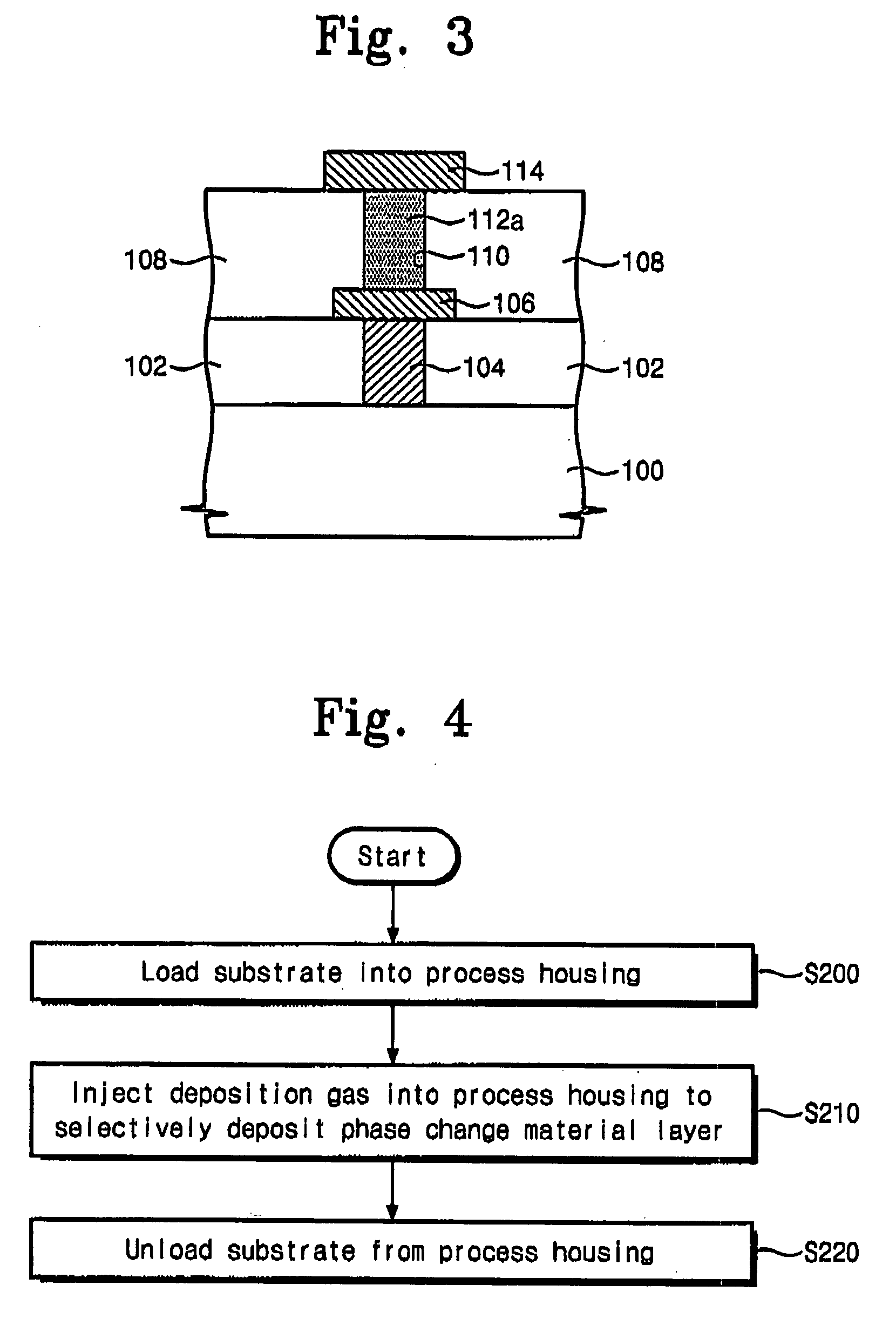
[0061]FIG. 5 illustrates a flowchart of a method of forming a phase change memory device according to the present invention. Referring to FIGS. 2, 5 and 6, the substrate 100 having the hole 110 exposing the lower electrode 106 may be loaded into the process housing 400 (S300). Herein, the substrate 100 may be loaded on the top surface of the chuck 405.

[0062]Referring to FIG. 5, the deposition gas may be supplied as a plurality of source gases that are grouped into a plurality of gas groups each having at least one source gas. In this embodiment, the deposition gas may contain a first, a second and a third group of gases. In other implementations, the deposition gas may include two gas groups, four gas groups, or more. Where the phase change material layer 112 is a GST, one of GeH(i-Bu)3, Sb(i—Pr)3, and Te(t-Bu)2 may be in the first gas group, another one of them may be in the second gas group, and the remaining one of them may be in the third gas group. A first gas group of the depo...

fourth embodiment

[0075]FIGS. 8 through 10 illustrate cross-sectional views of stages in a method of forming a lower electrode according to the present invention. Referring to FIG. 8, the lower insulating layer 102 may be formed on the substrate 100, and the lower plug 104 may be formed through the lower insulating layer 102. A buffer layer 105 may be formed on the lower insulating layer 102. The buffer layer 105 may be formed of a conductive material.

[0076]The interlayer insulating layer 108 may be formed on the surface of the substrate 100 and may be patterned so as to form the hole 110 exposing a region of the buffer layer 105. The buffer layer 105 may allow for increasing an alignment margin between the hole 110 and the lower plug 104. Accordingly, depending on the requirements of the particular device and fabrication process, the buffer layer 105 may be omitted, in which case the hole 110 may expose the lower plug 104.

[0077]As shown in FIG. 8, a preliminary lower electrode 107 in the shape of a ...


PUM

PropertyMeasurementUnit
temperatureaaaaaaaaaa
aspect ratioaaaaaaaaaa

Abstract

A method of forming a phase change material layer includes preparing a substrate having an insulator and a conductor, loading the substrate into a process housing, injecting a deposition gas into the process housing to selectively form a phase change material layer on an exposed surface of the conductor, and unloading the substrate from the process housing, wherein a lifetime of the deposition gas in the process housing is shorter than a time the deposition gas takes to react by thermal energy.

Description

BACKGROUND OF THE INVENTION[0001]1. Field of the Invention[0002]Embodiments of present invention relate to a method of forming a phase change material layer, a method of forming a phase change memory device using the same, and a phase change memory device so formed. More particularly, embodiments of the present invention relate to a method of forming a phase change material layer, a method of forming a phase change memory device using the same, and a phase change memory device so formed that may reduce or eliminate the formation of voids or seams in a phase change material layer.[0003]2. Description of the Related Art[0004]Among semiconductor devices, a phase change memory device has a nonvolatile characteristic, such that stored data are not lost even if a supply of power is interrupted. The phase change memory device may employ a phase change material layer that may exhibit two stable states for storing data. The phase change material layer may be transformed into amorphous state ...

Claims


Application Information

Patent Timeline
Patent Type & Authority Applications(United States)
IPC IPC(8): H01L27/10
CPCC23C16/305C23C16/45523H01L45/06H01L45/1683H01L45/126H01L45/144H01L45/1616H01L45/1233H10N70/8413H10N70/231H10N70/023H10N70/066H10N70/8828H10N70/826
Inventor CHO, SUNG-LAELEE, CHOONG-MANLEE, JIN- ILLIM, SANG-WOOKPARK, HYE-YOUNGPARK, YOUNG-LIM
Owner SAMSUNG ELECTRONICS CO LTD
Why Eureka
Try Eureka