Plasma etch reactor with distribution of etch gases across a wafer surface and a polymer oxidizing gas in an independently fed center gas zone

a technology of etch reactor and etch gas, which is applied in the direction of electric discharge tubes, electric lighting sources, electric discharge lamps, etc., can solve the problems of unavoidable non-uniform radial distribution of etch rate and profile across the wafer surface, exacerbate problems, and worsen the non-uniformity of etch ra

Active Publication Date: 2007-10-25
APPLIED MATERIALS INC
View PDF43 Cites 241 Cited by
  • Summary
  • Abstract
  • Description
  • Claims
  • Application Information

AI Technical Summary

Problems solved by technology

Such a nonuniform radial distribution of etch rate and profile across the wafer surface has appeared to be unavoidable for a number of reasons.
These problems are exacerbated when attempting to increase the etch rate by the expedient of increasing the process gas flow rate into the reactor chamber.
Such an increase in gas flow rate does not solve the problem of non-uniform residency time across the wafer surface (and hence the non-uniform dissociation across the wafer surface), and may even worsen the problem, thereby worsening the etch rate non-uniformity.
However, such a technique is not enough since the polymer composition distribution across the wafer surface is not significantly changed.
Thus, there appears to be no solution to the problem.
Such problems have not been pronounced for many processes involving fluorocarbon or hydrocarbon etch process gases in a plasma etch reactor chamber.
However, we have found that these problems arise with great severity when using particular combinations of such gases that otherwise produce the best possible process results, such a

Method used


Image

  • Plasma etch reactor with distribution of etch gases across a wafer surface and a polymer oxidizing gas in an independently fed center gas zone
  • Plasma etch reactor with distribution of etch gases across a wafer surface and a polymer oxidizing gas in an independently fed center gas zone
  • Plasma etch reactor with distribution of etch gases across a wafer surface and a polymer oxidizing gas in an independently fed center gas zone

Examples


Embodiment Construction

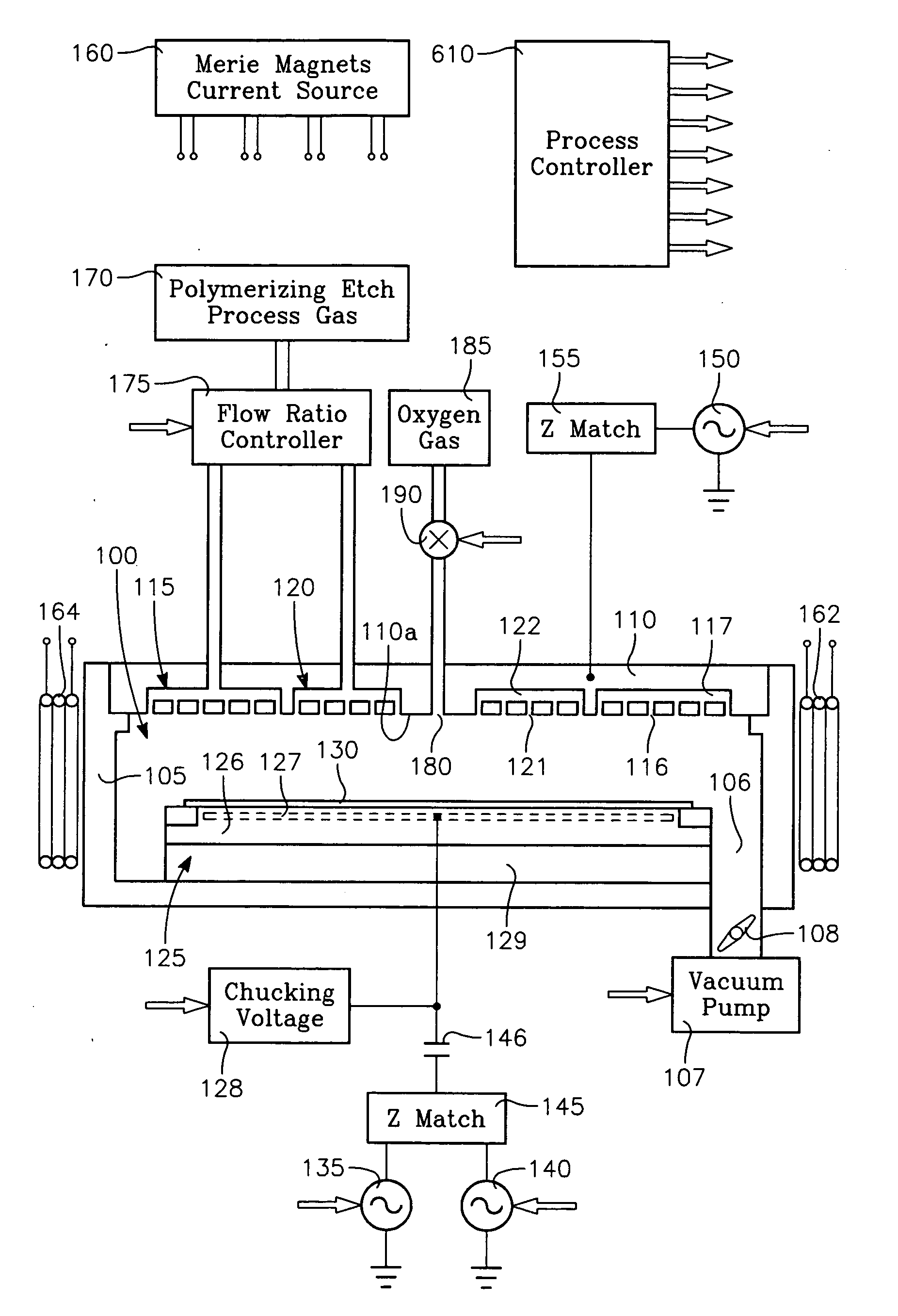
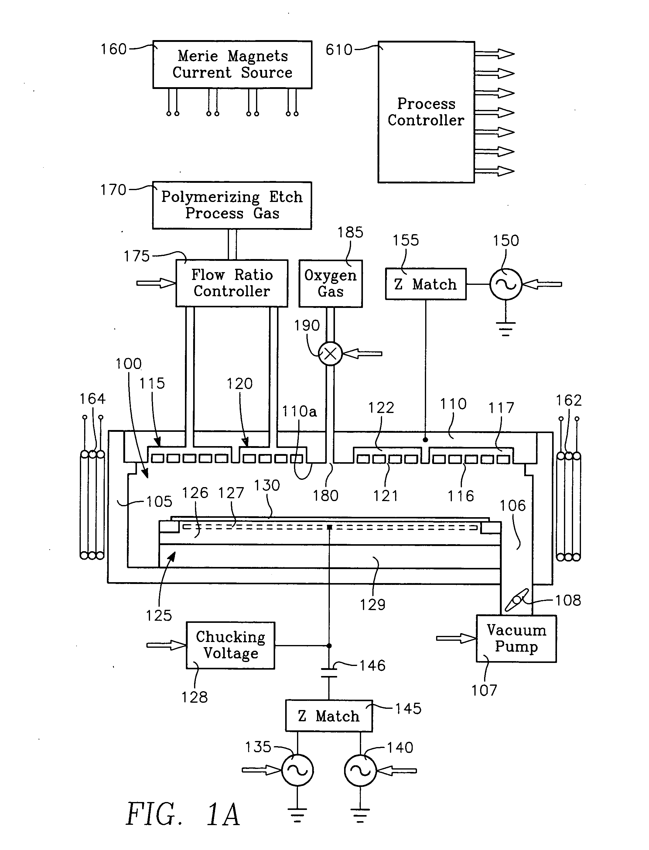
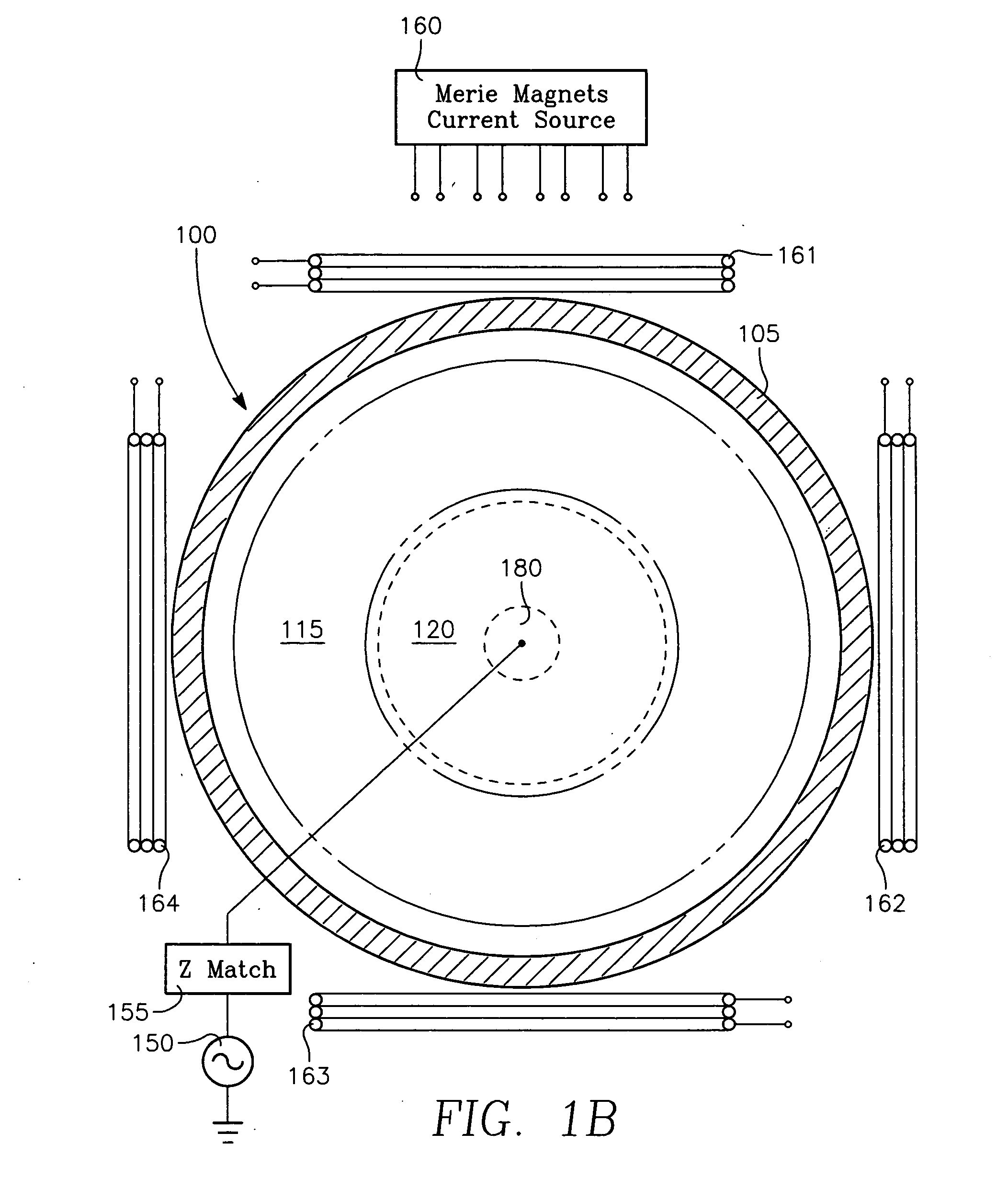
[0019]The present invention solves the problem of center-low etch rate and tapered etch profile at the wafer center that has plagued capacitively coupled plasma etch processes for etching dielectric thin films. The invention is based upon our surprising discovery that the problem can be completely solved without requiring any increase in etch process gas flow rate over the wafer center. It is further based upon our discovery that removing or slowing deposition of polymer on sidewalls of narrow openings at the wafer center during the etch process is the only effective solution, rather than attempting to change the etch gas flow rate at the wafer center. Finally, the invention is based upon our surprising discovery that a gas such as oxygen which does not etch dielectric material, but which does reduce the amount of deposited polymer, is an essential part of this solution. Such a gas is referred to herein as a polymer-retarding gas. The invention is realized by providing a novel indep...


PUM

PropertyMeasurementUnit
Frequencyaaaaaaaaaa
Frequencyaaaaaaaaaa
Flow rateaaaaaaaaaa

Abstract

A plasma etch reactor for plasma enhanced etching of a workpiece such as a semiconductor wafer includes a housing defining a process chamber, a workpiece support configured to support a workpiece within the chamber during processing and comprising a plasma bias power electrode. The reactor further includes a first process gas inlet coupled to receive predominantly or pure oxygen gas and a second process gas inlet coupled to receive a polymerizing etch process gas. The reactor has a ceiling plasma source power electrode including a center circular gas disperser configured to receive a process gas from the first process gas inlet and to distribute the process gas into the chamber over the workpiece, and an inner annular gas disperser centered around the center gas disperser configured to receive the process gas from the second process gas inlet and to distribute the process gas into the chamber over the workpiece through an inner plurality of injection ports.

Description

BACKGROUND OF THE INVENTION[0001]Fabrication of integrated circuits with feature sizes on the order of nanometers requires etch processes that are extremely uniform across the entire surface of a semiconductor wafer, typically about 300 millimeters in diameter. Such uniform etch processes are typically realized in a plasma etch reactor such as a capacitively coupled plasma reactor with an overhead electrode having a high aspect ratio (e.g., an electrode-to-wafer gap of only 2.5 cm for a 300 mm wafer). The etch process gas, which may be a fluorocarbon or fluorohydrocarbon gas, is of the type that forms a protective polymer layer over photoresist or other thin film surfaces that are not to be etched. Such a protective thin film also forms on the opening sidewalls formed during the etch process. Formation of such a protective polymer layer enhances etch selectivity and provide the means for etch profile control.[0002]Such processes exhibit a low etch rate and / or tapered etch profile (d...

Claims


Application Information

Patent Timeline
IPC IPC(8): C23F1/00
CPCH01J37/3244H01J37/321
Inventor KIM, JONG MUNLIU, JINGBAOPU, BRYAN Y.
Owner APPLIED MATERIALS INC
Why Eureka
Try Eureka