Active matrix emissive display and optical scanner system, methods and applications

a technology of active matrix and optical scanner, applied in static indicating devices, acquiring/reconfiguring fingerprints/palmprints, instruments, etc., can solve the problems of reducing sensitivity, limiting the size and brightness of light emitting pixels, and small commercial eds

Inactive Publication Date: 2007-11-01
KONICEK JEFFREY C
View PDF98 Cites 71 Cited by
  • Summary
  • Abstract
  • Description
  • Claims
  • Application Information

AI Technical Summary

Benefits of technology

[0013]It is another object of the invention to provide an active matrix ED display / scanner combination that would allow each pixel to operate as a light source or a light detector, and when acting as a light source, be able to be decoupled from the display's drivers but still illuminate.
[0019]It is another object of the invention to create a fingerprint scanner that can more readily discern between a scan of a real fingerprint and a scan of a picture or image of a fingerprint.
[0024]It is another object of the invention to provide an optically sensing display that is configured to sense impinging light on the display, and as a result, to extend the battery life of portable electronic devices by automatically dimming the intensity of the display in low ambient lighting conditions. It is another object of the invention to create an active matrix display capable of being an input device for a computer, cell phone, digital camera, PDA, television or other electronic device having a display.
[0026]It is another object of the invention to create a better credit card, debit card, or smart card capable of greater security and privacy.
[0030]It is another object of the invention to provide active matrix ED that both displays data and optically scans the external lighting environment while minimizing image-perturbation by adjusting the scanning technique so that sequential columns (or rows) are not scanned, and instead the display is scanned in a pseudo-random way or by otherwise variably scanning only selected portions of the display.

Problems solved by technology

Currently, commercial EDs are relatively small and primarily based on passive technology, which is basically an array of overlapping conductors running in an X and Y direction.
US Patent Application Publication 2005 / 0231656 (incorporated herein by reference), has an image sensor having photosensitive TFT transistors in an array, but wherein the TFT devices themselves are not capable of generating or modulating light.
One problem with the existing emissive display / optical scanner combination is that it is based on passive display technology, which limits its size and to some extent the brightness of the light emitting pixels (because of the need to multiplex the drivers to the pixels).
The problem with existing light sensing LCD display technology is that it relies on the small (relative to the pixel size) TFT transistor to be the light sensing device and relies on ambient lighting to be the light source.
The TFT transistor that receives the light for detection is susceptible to detecting internal reflections of the display's backlighting from the LCD material, and is generally not placed in an optimal position within the pixel window.
Further, the optical TFT is usually beneath the LCD material and off to one side of the pixel, thus, reducing sensitivity.

Method used


Image

  • Active matrix emissive display and optical scanner system, methods and applications
  • Active matrix emissive display and optical scanner system, methods and applications
  • Active matrix emissive display and optical scanner system, methods and applications

Examples


Embodiment Construction

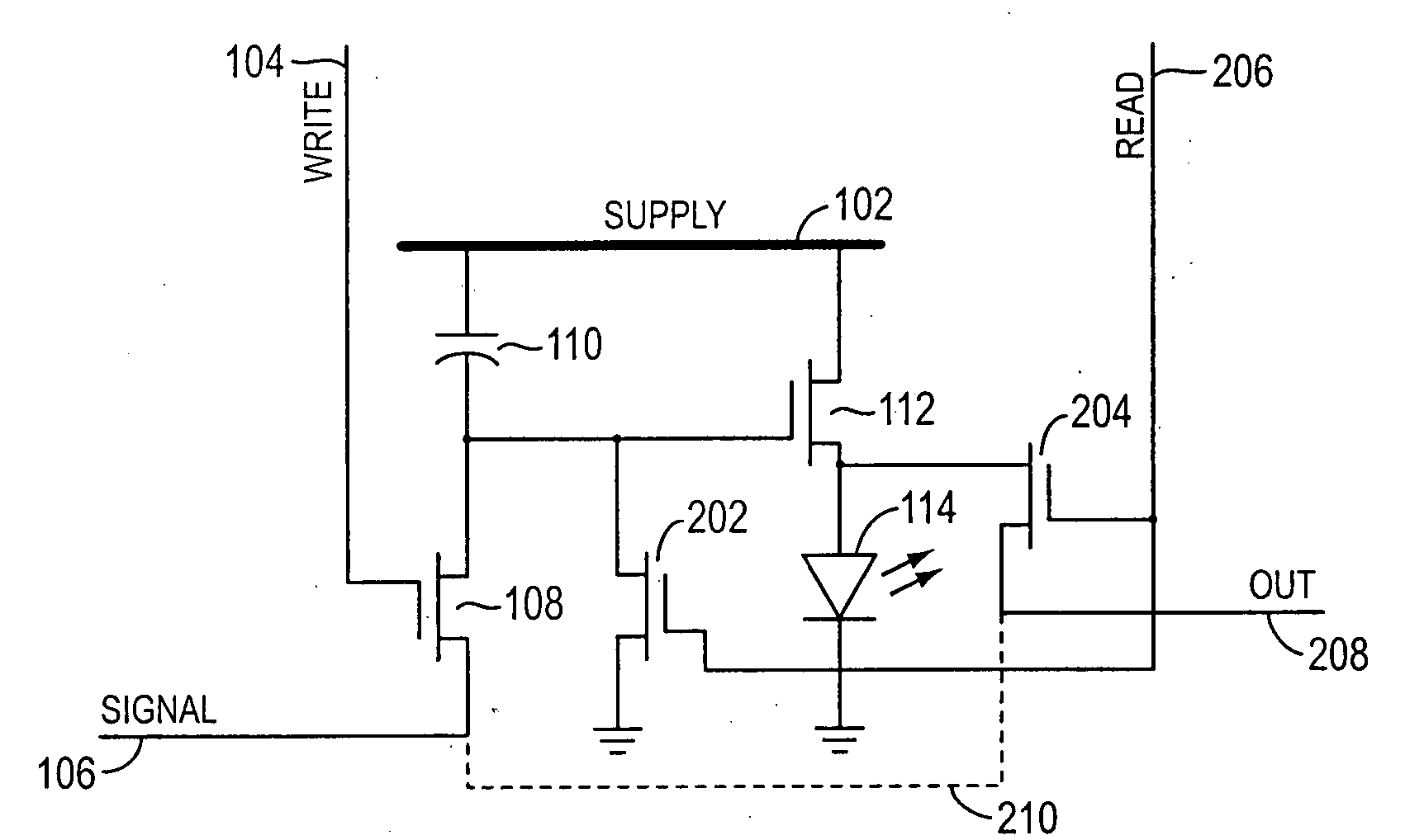
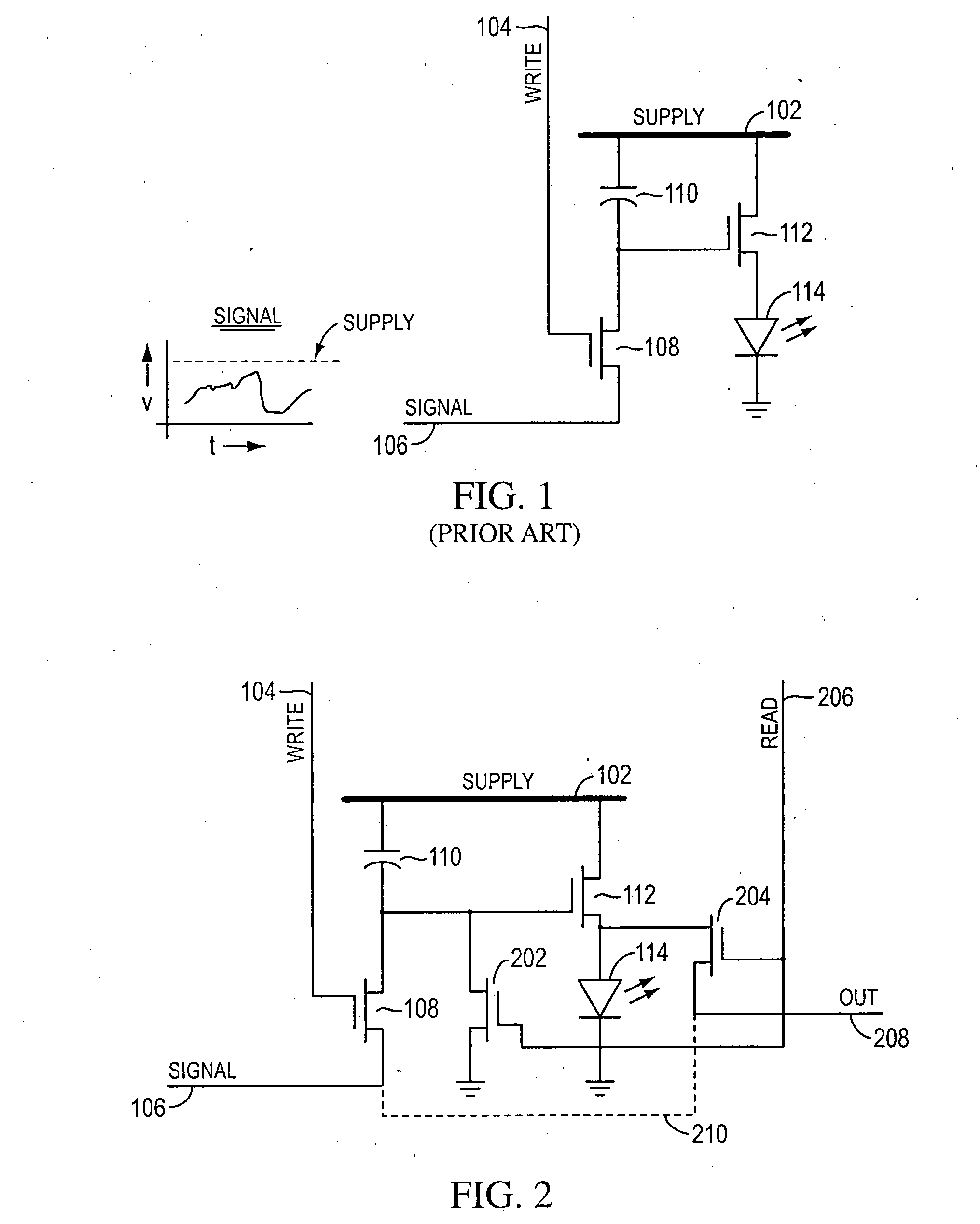
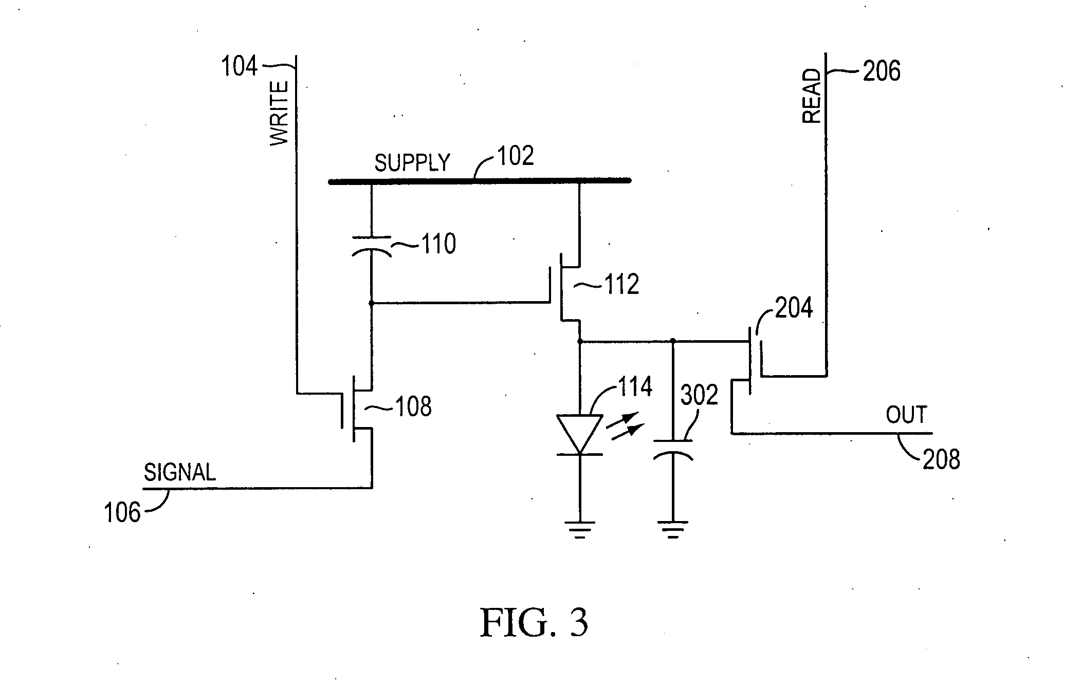
[0047]In my co-pending application, “Flat Panel Display Screen Operable for Touch Position Determination”, Ser. No. 11 / 378,205, filed Mar. 17, 2006, herein incorporated by reference, is disclosed a preferred modification to a typical ED pixel (see, e.g., FIGS. 6 and 7 of that application) which allows electrical access to the anode of a common-cathode LED in the pixel. This modification, as will be shown in greater detail below, forms a preferred basis for an active matrix ED display scanner combination.

[0048]FIG. 1 shows a typical ED pixel in schematic form. This schematic is provided in a relatively simple form, and other equivalent circuits are considered within the scope of the invention. Thus, the invention may be applied to any specific form of relatively low voltage emissive display (ED) technology, including those based on organic LED (OLED), polymer LED (PLED), quantum dot, etc. Again, those skilled in the art are directed to the materials incorporated by reference above fo...


PUM


Abstract

An active matrix emissive display (ED) is disclosed that also includes optical scanning capability. Each display pixel is independently addressable and independently internally driven for light generation. Each display pixel is also given the ability to be coupled to detection circuitry in order to sense currents or voltages that are optically generated or leaked by its internal LED when exposed to light (and thus acting in a photodiode capacity). Since the intensity of the light illuminating the diode determines the magnitude of generated currents and / or voltages or leakage current through the diode (when reverse biased), these sensed currents or voltages give an indication of the intensity of the light striking the pixel. In this manner, active matrix ED pixels are configured to serve the dual purpose of being able to generate and detect light.

Description

CROSS-REFERENCE TO RELATED APPLICATION[0001]This application claims the benefit of U.S. Provisional Application No. 60 / 797,015, filed May 1, 2006, which is herein incorporated by reference in its entirety.BACKGROUND OF THE INVENTION[0002]Low voltage emissive display (ED) technology based on organic LED (OLED), polymer LED (PLED), quantum dot, etc. offers great promise for improving display technology. EDs are beginning to appear on the market and break into the once-dominating LCD display technology for such things as portable electronic devices, computers, TVs, etc.[0003]Currently, commercial EDs are relatively small and primarily based on passive technology, which is basically an array of overlapping conductors running in an X and Y direction. At each point of overlap between an X and Y conductor, sandwiched between the two conductors, is a layer of emissive material such that when current is driven through one X conductor and received at a Y conductor, the emissive material at th...

Claims


Application Information

Patent Timeline
Patent Type & Authority Applications(United States)
IPC IPC(8): G06K7/00
CPCG06K9/0004G06K9/0012G06K9/00899G09G3/3233G09G2360/148G09G2320/064G09G2330/021G09G2360/144G09G2300/0866G06V40/1318G06V40/1394G06V40/40
Inventor KONICEK, JEFFREY C.
Owner KONICEK JEFFREY C
Why Eureka
Try Eureka