Improved CMOS diodes with dual gate conductors, and methods for forming the same

a technology of complementary metaloxidesemiconductor and diode, which is applied in the direction of diodes, semiconductor devices, semiconductor/solid-state device details, etc., can solve the problems of significant overlay misalignment and critical dimension (cd) variations, deleterious electric field variation at the diode interface, etc., and achieve the effect of reducing variations and advantageously reducing ideality factor variations in such improved cmos diodes

Inactive Publication Date: 2007-11-01
GLOBALFOUNDRIES INC
View PDF24 Cites 26 Cited by
  • Summary
  • Abstract
  • Description
  • Claims
  • Application Information

AI Technical Summary

Benefits of technology

[0011] The present invention provides improved CMOS diodes with dual gate conductors, one of which is doped with n-type dopant species and the other is doped with p-type dopant species. The widths of the P+ / N+ doped regions in such dual gate conductors are determined by a gate patterning process, instead of the error-prone masked dopant implantation process, and therefore have significantly reduced variations. Consequently, the ideality factor variations in such improved CMOS diodes are advantageously reduced.

Problems solved by technology

However, doping of the first and second portions 122 and 124 of the single gate conductor is typically achieved by masked dopant implantation, which, due to limitations of the lithographic tools used, can result in significant overlay mis-alignment and critical dimension (CD) variations.
Consequently, the widths of the accumulation region 116 and the depletion region 118 may vary significantly, which in turn leads to deleterious electric field variation at the diode interface.

Method used


Image

  • Improved CMOS diodes with dual gate conductors, and methods for forming the same
  • Improved CMOS diodes with dual gate conductors, and methods for forming the same
  • Improved CMOS diodes with dual gate conductors, and methods for forming the same

Examples


Embodiment Construction

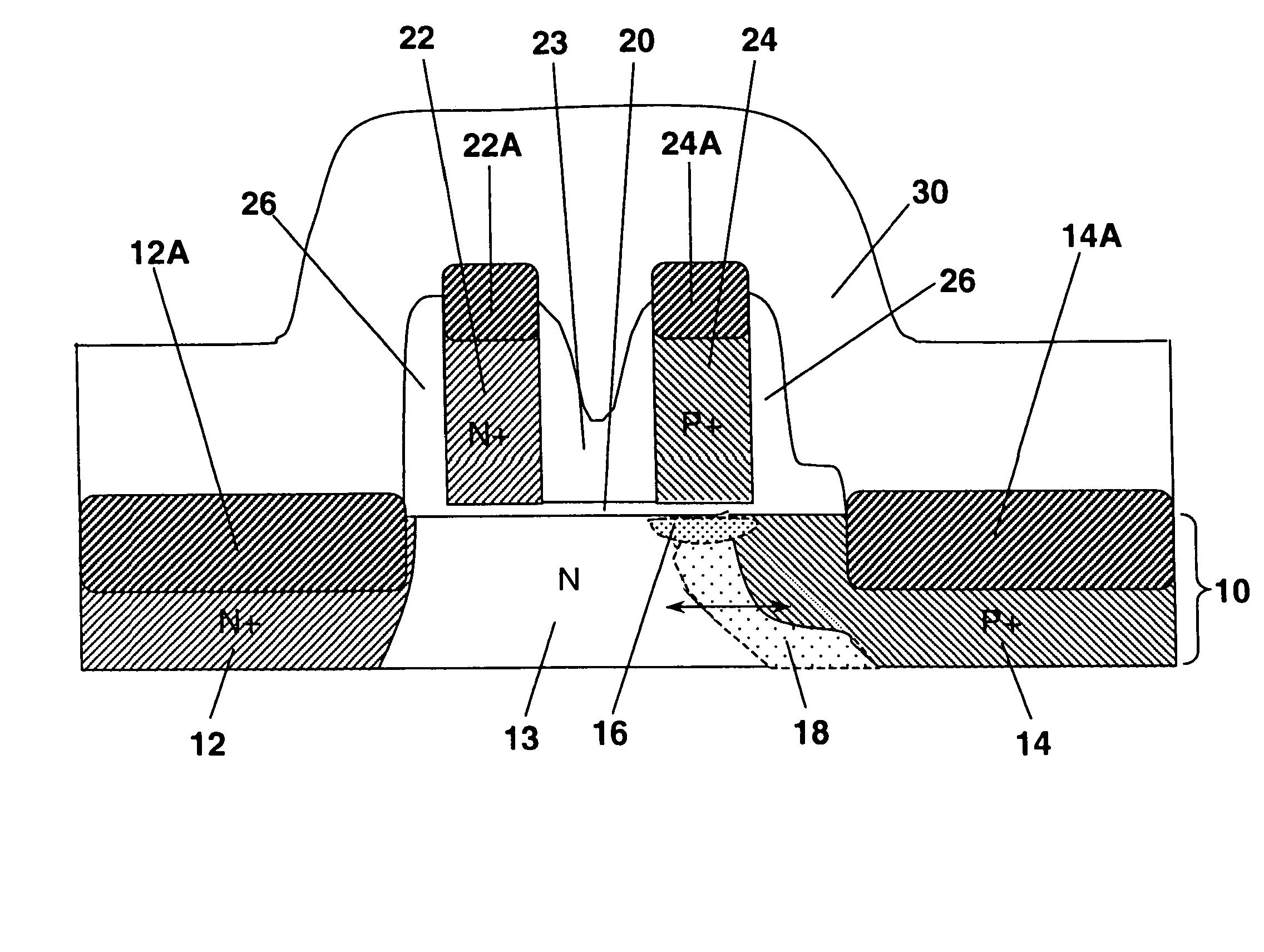
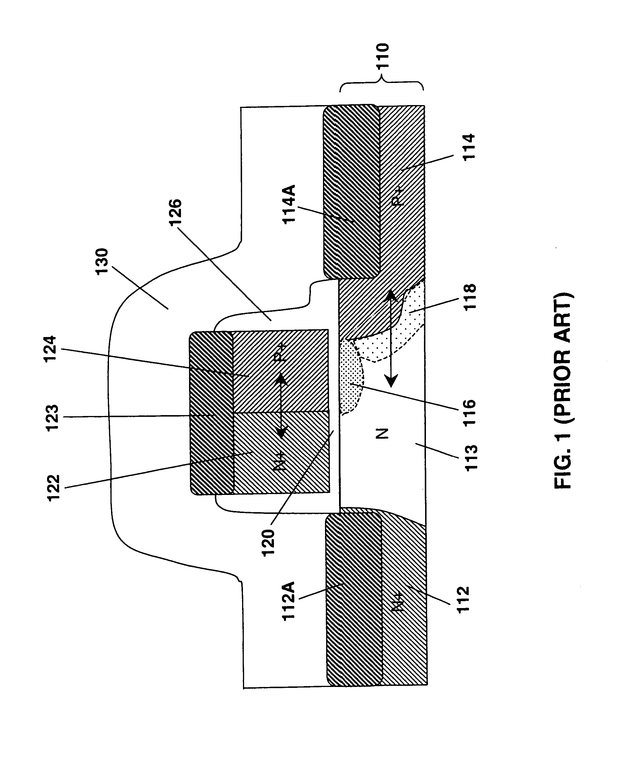
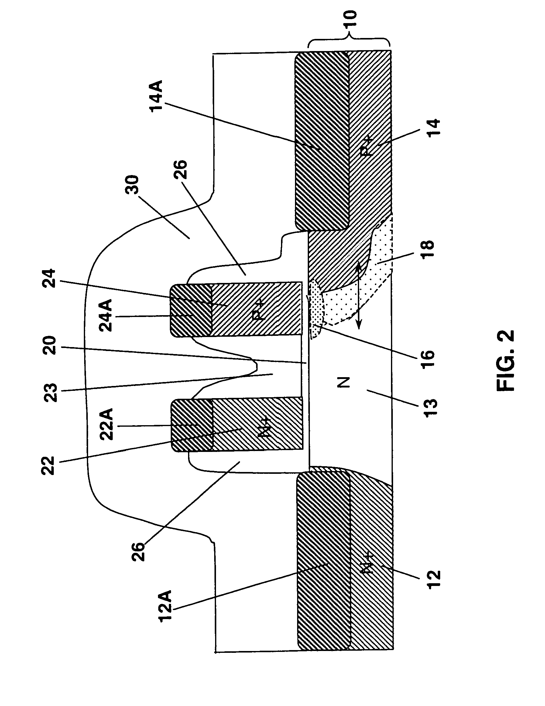
[0047] In the following description, numerous specific details are set forth, such as particular structures, components, materials, dimensions, processing steps and techniques, in order to provide a thorough understanding of the present invention. However, it will be appreciated by one of ordinary skill in the art that the invention may be practiced without these specific details. In other instances, well-known structures or processing steps have not been described in detail in order to avoid obscuring the invention.

[0048] It will be understood that when an element as a layer, region or substrate is referred to as being “on” or “over” another element, it can be directly on the other element or intervening elements may also be present. In contrast, when an element is referred to as being “directly on” or “directly over” another element, there are no intervening elements present. It will also be understood that when an element is referred to as being “beneath” or “under” another elem...


PUM


Abstract

The present invention provides an improved CMOS diode structure with dual gate conductors. Specifically, a substrate comprising a first n-doped region and a second p-doped region is formed. A third region of either n-type or p-type conductivity is located between the first and second regions. A first gate conductor of n-type conductivity and a second gate conductor of p-type conductivity are located over the substrate and adjacent to the first and second regions, respectively. Further, the second gate conductor is spaced apart and isolated from the first gate conductor by a dielectric isolation structure. An accumulation region with an underlying depletion region can be formed in such a diode structure between the third region and the second or the first region, and such an accumulation region preferably has a width that is positively correlated with that of the second or the first gate conductor.

Description

FIELD OF THE INVENTION [0001] The present invention relates to improved complementary metal-oxide-semiconductor (CMOS) diode structures. More specifically, the present invention relates to CMOS diodes having dual gate conductors, which function to reduce the P+ / N+ variation and the ideality variation of the CMOS diodes. BACKGROUND OF THE INVENTION [0002] A diode is a critical device in CMOS technology, which can be used in bandgap reference circuits. FIG. 1 shows a conventional CMOS diode formed in a semiconductor substrate 110. The semiconductor substrate 110 comprises a first region 112 that has n-type conductivity and a second region 114 that has p-type conductivity. The first and second regions 112 and 114 jointly define a third region 113 located therebetween in the semiconductor substrate 110, which has either n-type or p-type conductivity, but at a significantly lower dopant concentration in comparison with the first or second regions 112 or 114. The first and second regions ...

Claims


Application Information

Patent Timeline
Patent Type & Authority Applications(United States)
IPC IPC(8): H01L23/62
CPCH01L29/7391H01L29/66356
Inventor ONSONGO, DAVID M.RAUSCH, WERNERYANG, HAINING S.
Owner GLOBALFOUNDRIES INC
Why Eureka
Try Eureka