Method for fabricating polarization reversal structure and reversal structure

a technology of polarization reversal and polarization reversal, which is applied in the direction of light demodulation, instruments, optical waveguide light guides, etc., can solve the problems of damage generated at the forward end of comb electrodes, and achieve the effect of preventing damage onto the substrate and low resistan

Active Publication Date: 2007-11-08
NGK INSULATORS LTD +1
View PDF4 Cites 2 Cited by
  • Summary
  • Abstract
  • Description
  • Claims
  • Application Information

AI Technical Summary

Benefits of technology

[0010] That is, each electrode portion of the comb electrode corresponds with each inversion part of the domain inversion structure one by one, so that a gap is formed between adjacent electrode portions. Contrary to this, according to the present invention, each electrode portion itself is separated to electrode pieces in the direct

Problems solved by technology

According to prior methods, however, when it is tried to obtain periodic domain inversion structure having a period of, for exampl

Method used


Image

  • Method for fabricating polarization reversal structure and reversal structure
  • Method for fabricating polarization reversal structure and reversal structure
  • Method for fabricating polarization reversal structure and reversal structure

Examples


experiment 1

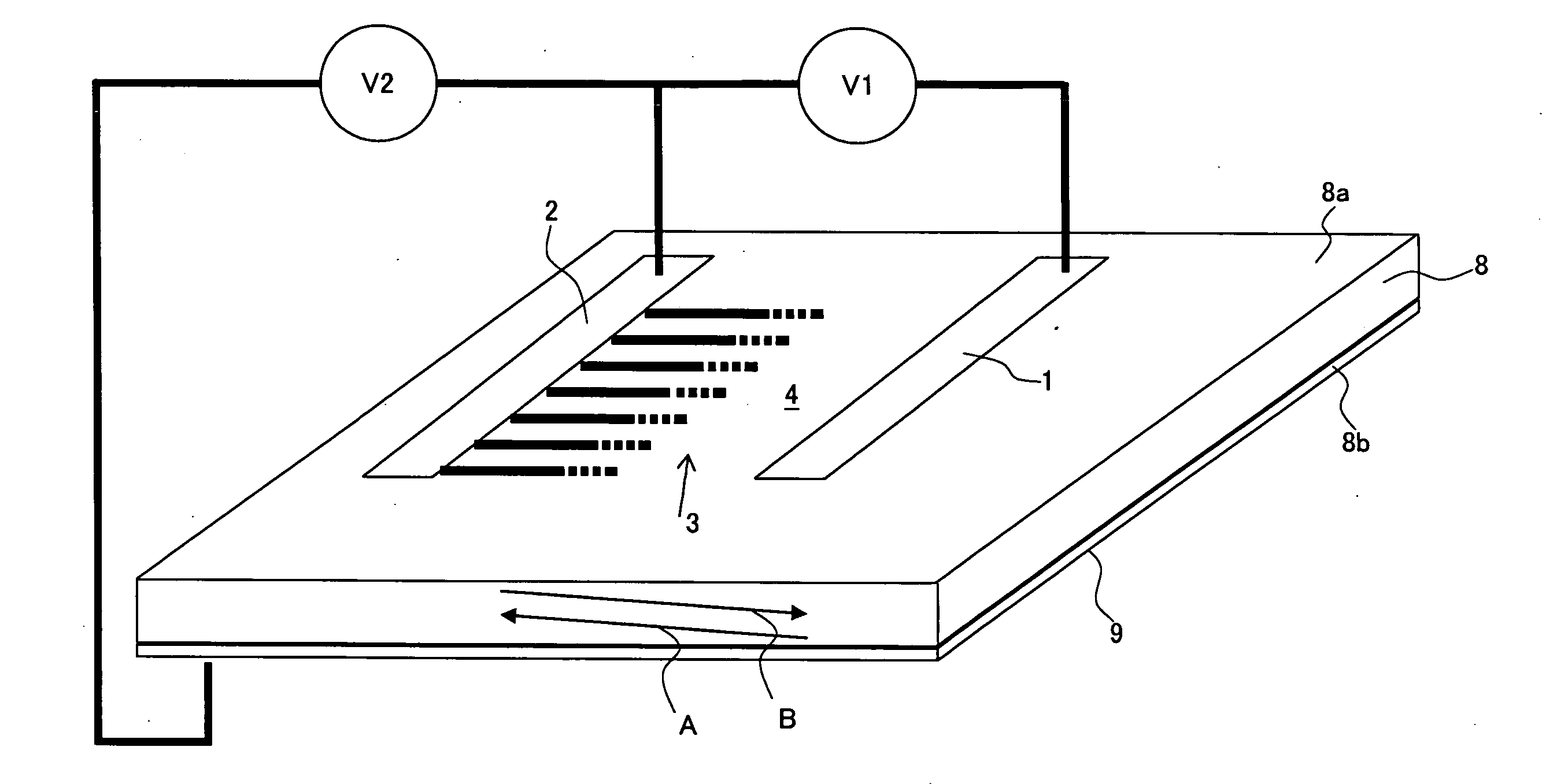
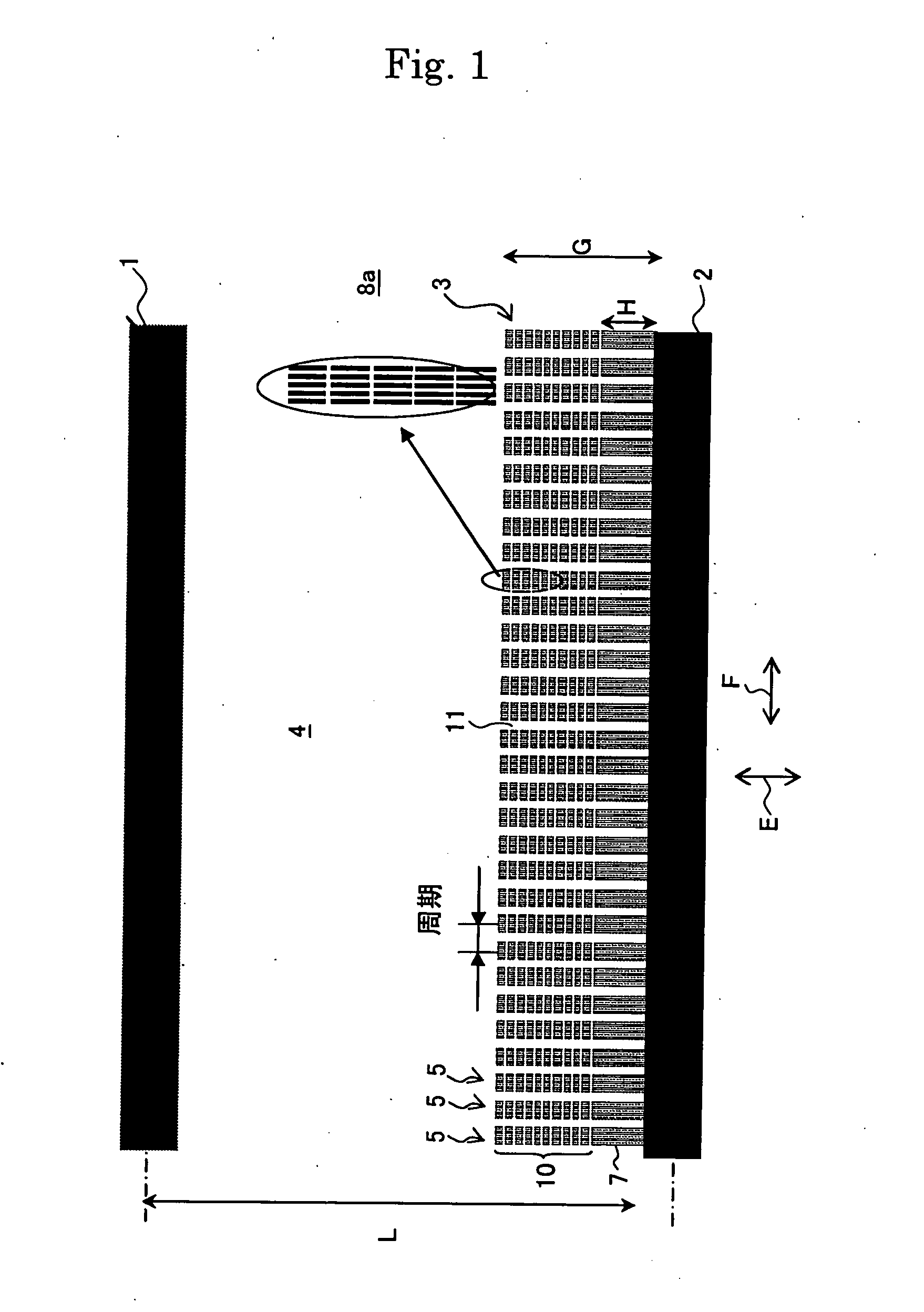
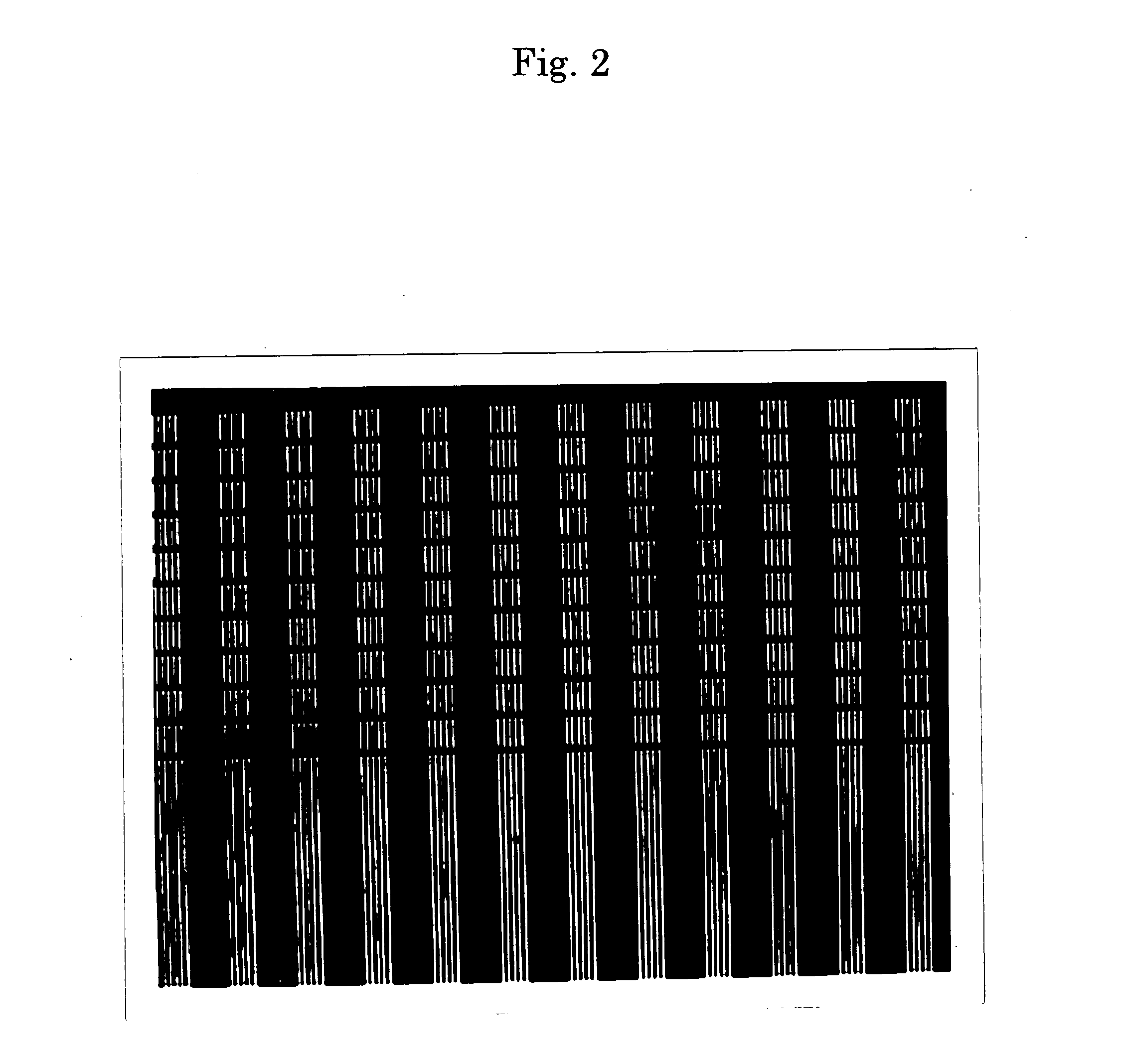
[0048] Periodic polarization inversion structure was formed by electric field poling process, according to the process described referring to FIGS. 1 to 3 and 5. The distance “L” between the feeding portion 2 and opposing electrode 1 was made 400 μm, the period of domain inversion was made 18 μm, the whole length “G” of the electrode portion 5 was made 150 μm, the height “H” of the base portion 7 was made 60 μm, the number of the gaps “C” in the direction “E” was made 10 (11 arrays), the number of the gaps “D” in the direction “F” was made 4 (5 arrays), the gap “C” was made 1 μm and the gap D was made 0.5 μm. FIG. 2 is a photograph showing an enlarged view of the comb electrode actually patterned. According to this example, Ta metal was used for the patterning.

[0049] The electrode pattern was formed on the surface of the substrate, and the uniform electrode was patterned onto the back face of the substrate. A voltage was applied according to the pattern shown in FIG. 5. Further, al...

example 2

[0058] The domain inversion structure was formed according to the same procedure as the example 1. However, the pattern of the comb electrode was shown in FIG. 4 and the gaps in the direction of the arrow “E” were not formed. As a result, it was obtained the shape of a constant width from the forward end toward the root of the electrode and cracks were not generated.


PUM


Abstract

When a domain inversion part is produced by means of electric field polling process, damage in the vicinity of the forward end of a comb electrode and deviation of width of each domain inversion part are to be reduced. A polarization domain inversion structure has polarization domain inversion parts is produced by electric field poling process using a comb electrode formed on one surface of a substrate of a ferroelectric single crystal and of a single domain, and the comb electrode has a plurality of electrode portions and feeding portion. Each of the electrode portions corresponds with each domain inversion part of the domain inversion structure. The electrode portion has a plurality of low resistance pieces arranged in a direction “F” intersecting the longitudinal direction “E” of the electrode portion and spaced apart with each other.

Description

FIELD OF THE INVENTION [0001] The invention relates to a method of producing polarization inversion parts by means of electric field poling process. BACKGROUND OF THE INVENTION [0002] Periodic domain inversion structure can be formed in a ferroelectric and non-linear optical crystal such as lithium niobate or lithium tantalite so as to generate second harmonic wave corresponding with the period. An optical waveguide can be easily formed in such crystals as lithium niobate or lithium tantalate, so that a device for generating second harmonic wave of high efficiency and small size can be provided. It is possible to generate light of a wavelength of ultraviolet, visible and infrared regions only with an excitation laser oscillating fundamental wave. The device can be applied in a wide variety of applications such as medical use, opt-chemical use and various kinds of optical measurement. [0003] It is necessary to form deep polarization inversion structure in a ferroelectric single cryst...

Claims


Application Information

Patent Timeline
IPC IPC(8): G02F1/35
CPCG02F1/3558
Inventor YAMAGUCHI, SHOICHIROIWATA, YUICHISUZUKI, KENGO
Owner NGK INSULATORS LTD
Why Eureka
Try Eureka