

Printed circuit board and method of manufacturing printed ciruit board
a printed circuit board and circuit board technology, applied in the field of printed circuit boards, can solve the problems of insufficient effect of chip capacitors, inability to reduce wiring inductance as currently desired in the higher frequency region of ic chips, and inability to achieve the effect of enhancing the connection characteristics, and reducing the probability of defective printed circuit boards
- Summary
- Abstract
- Description
- Claims
- Application Information
AI Technical Summary
Benefits of technology
Problems solved by technology
Method used
Image

Examples
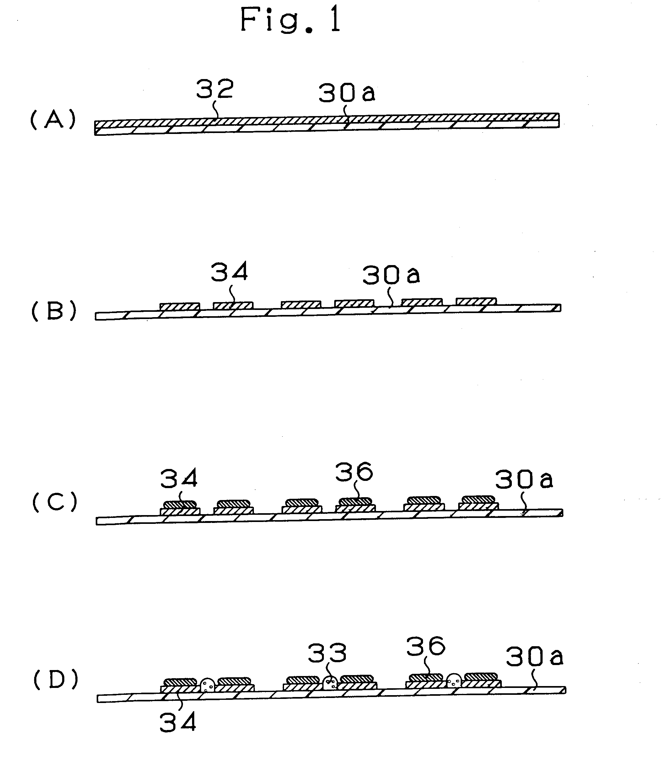
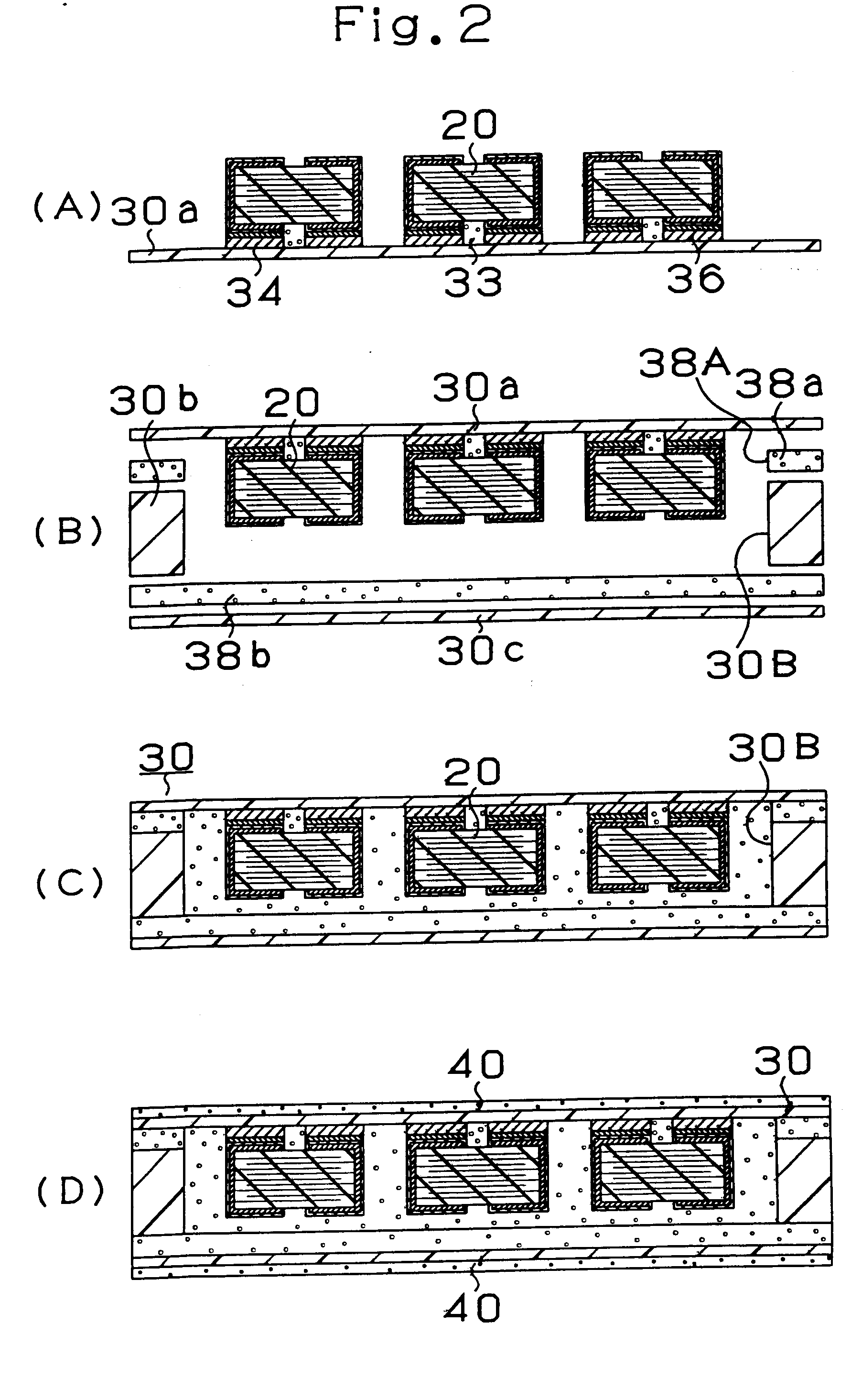
first embodiment
First Other Example of First Embodiment
[0220] A printed circuit board according to the first other example of the first embodiment of the present invention will be described hereinafter with reference to FIG. 9. The printed circuit board in the first other example of the first embodiment is almost the same as the printed circuit board in the first embodiment stated above. However, in the printed circuit board in the first other example, conductive connection pins 96 are provided at the printed circuit board and the printed circuit is connected to a daughter board through the conductive connection pins 96.
[0221] Further, in the first embodiment stated above, only the chip capacitors 20 contained in the core substrate 30 are provided. In this example, mass storage chip capacitors 86 are mounted on the front and reverse sides of the substrate.
[0222] The IC chip momentarily consumes high power and performs complex arithmetic operation. In the first other example, to supply high power ...
second embodiment
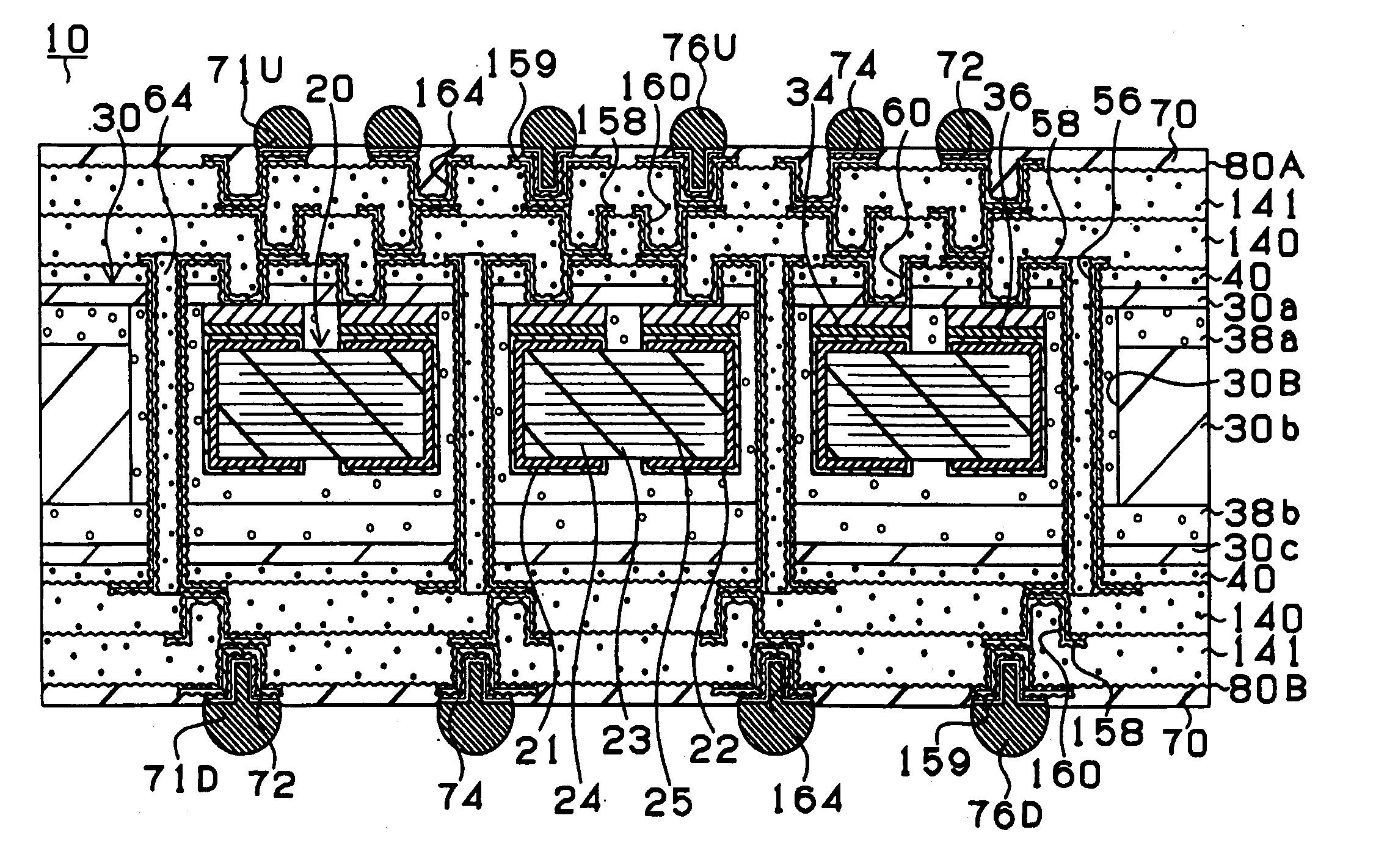
[0248] The constitution of a printed circuit board according to the second embodiment of the present invention will be described hereinafter with reference to FIGS. 19 and 20. FIG. 19 is a cross-sectional view of a printed circuit board 210. FIG. 20 shows a state in which an IC chip 290 is mounted on the printed circuit board 210 shown in FIG. 19 and that the printed circuit board 210 is attached to a daughter board 295.
[0249] As shown in FIG. 19, the printed circuit board 210 consists of a core substrate 230 containing a chip capacitor 220, and buildup wiring layers 280A and 280B. The buildup wiring layers 280A and 280B are connected to each other by through holes 256. Each of the wiring layers 280A and 280B consists of interlayer resin insulating layers 240 and 340. At the upper buildup wiring layer 280A side, conductor circuits 358 and via holes 260 connected to the first electrode 221 and the second electrode 222 of the chip capacitor 220, respectively, are formed on the interl...
third embodiment
First Other Example of Third Embodiment
[0331] A printed circuit board according to the first other example of the third embodiment of the present invention will be described hereinafter with reference to FIG. 32. The printed circuit board in the first other example is almost the same as the printed circuit board in the third embodiment stated above. However, in the printed circuit board in the first other example, conductive connection pins 496 are provided at the printed circuit board and the printed circuit is connected to a daughter board through the conductive connection pins 496.
[0332] Further, in the third embodiment stated above, only the chip capacitors 420 contained in the core substrate 430 are provided. In this example, mass storage chip capacitors 486 are mounted on the front and reverse sides of the substrate.
[0333] The IC chip momentarily consumes high power and performs complex arithmetic operation. In the first other example, to supply high power to the IC chip, ch...
PUM
 Abstract
Description
Claims
Application Information