

Display device and manufacturing method thereof
- Summary
- Abstract
- Description
- Claims
- Application Information
AI Technical Summary
Benefits of technology
Problems solved by technology
Method used
Image

Examples
Embodiment Construction
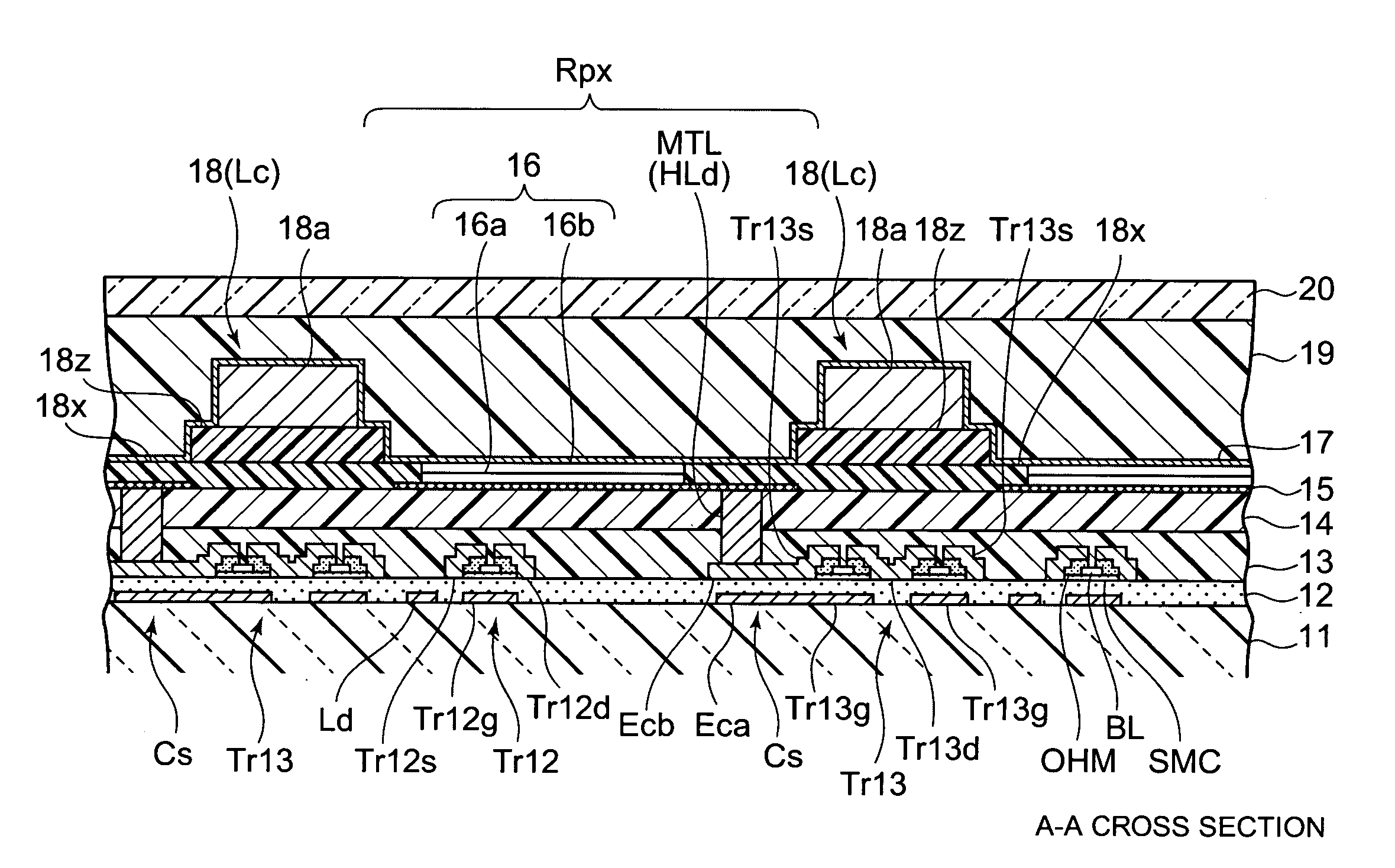
[0042]A display device and a manufacturing method thereof according to the present invention will be explained below in detail, by showing an embodiment. In the embodiment described below, such a case will be explained, in which an organic EL element having an organic EL layer including a high-molecular organic material described above is used as the light emitting element to constitute each pixel.
(Display Panel)
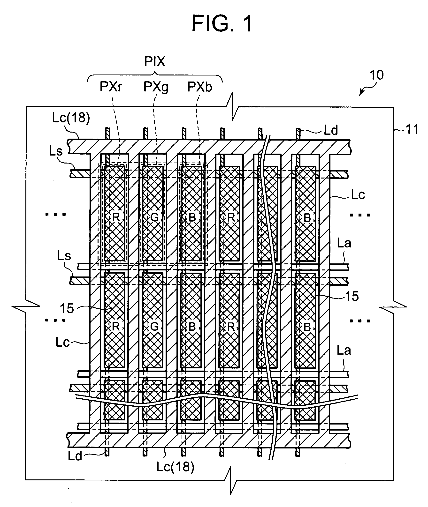
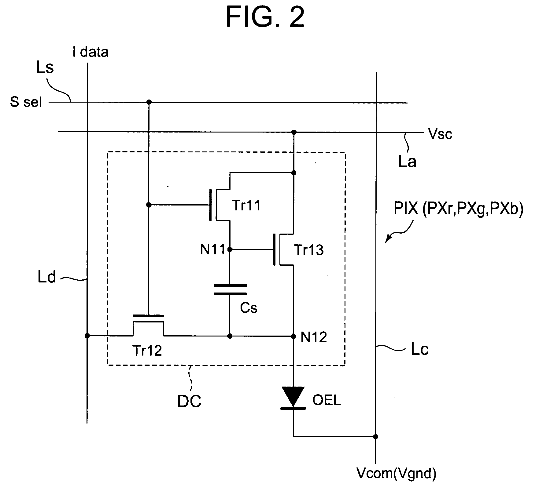
[0043]First, a display panel and pixels to be used in the display device according to the present invention will be explained.
[0044]FIG. 1 is a schematic plan view showing an example of an array of pixels on the display panel used on the display device according to the present invention. FIG. 2 is an equivalent circuit schematic showing an example of a circuit structure of each pixel (a display element and a pixel drive circuit) to be two-dimensionally arrayed on the display panel of the display device according to the present invention. To facilitate understanding, the plan...
PUM
| Property | Measurement | Unit |
|---|---|---|
| Electrical conductor | aaaaa | aaaaa |
| Photosensitivity | aaaaa | aaaaa |
Abstract
Description
Claims
Application Information