Integrated circuit chip packaging

a technology of integrated circuits and chip packaging, which is applied in the direction of printed circuit components, printed circuit manufacturing, instruments, etc., can solve the problems of signal distortion, higher manufacturing cost of buried circuits via b>110/b>, and signal subject to problems, so as to achieve low cost and high performance

Active Publication Date: 2007-11-15
IBM CORP
View PDF13 Cites 5 Cited by
  • Summary
  • Abstract
  • Description
  • Claims
  • Application Information

AI Technical Summary

Benefits of technology

[0015] The inventors of the present invention discovered that more direct access to a conductor that is embedded between layers of a printed circuit board is desired, without having to rely upon a surface mount or a via to connect to an embedded conductor.
[0017] An embedded conductor is superior to a surface conductor because an embedded conductor has better signal fidelity and an embedded conductor is completely shielded, while a surface conductor is not completely shielded. Therefore, an exemplary embodiment of the present invention is advantageous because the integrated circuit chips no longer need to connect to surface conductors, rather the integrated circuit chips may attach more directly to embedded conductors.
[0022] It is advantageous to minimize the length of a wire bond and / or a ribbon bond, because a bond represents a discontinuity. Therefore, milling the cavity such that the top of the chip is substantially co-planar with the launch, minimizes the length of a wire / ribbon bond and, as a result, reduces the adverse affects of the discontinuity.
[0028] Further, an exemplary embodiment of the present invention may be adapted to either wire / ribbon bonding or to a flip chip implemenation. This packaging technique offers even higher performance than the conventional techniques mentioned above while at the same time being low in cost.

Problems solved by technology

A surface attachment restricts the launch to a conductive layer that is on the surface of a printed circuit board and if a signal from the integrated circuit chip must be launched into a conductive layer that is between the layers of the printed circuit board (i.e., an embedded conductor), then the signal is subject to problems, which may be caused by vias that are used to transfer the signal from the surface to the embedded conductor.
However, a buried via 110 is more expensive to fabricate.
This configuration, referred to as a “through via,” minimizes the length of the stub, but the presence of the via still leads to signal distortion.
In addition, if many signals try to connect to embedded conductors at the same level of a layer, then wiring congestion may result.

Method used


Image

  • Integrated circuit chip packaging
  • Integrated circuit chip packaging
  • Integrated circuit chip packaging

Examples


Embodiment Construction

[0036] Referring now to the drawings, and more particularly to FIGS. 1-5, there are shown exemplary embodiments of the method and structures of the present invention.

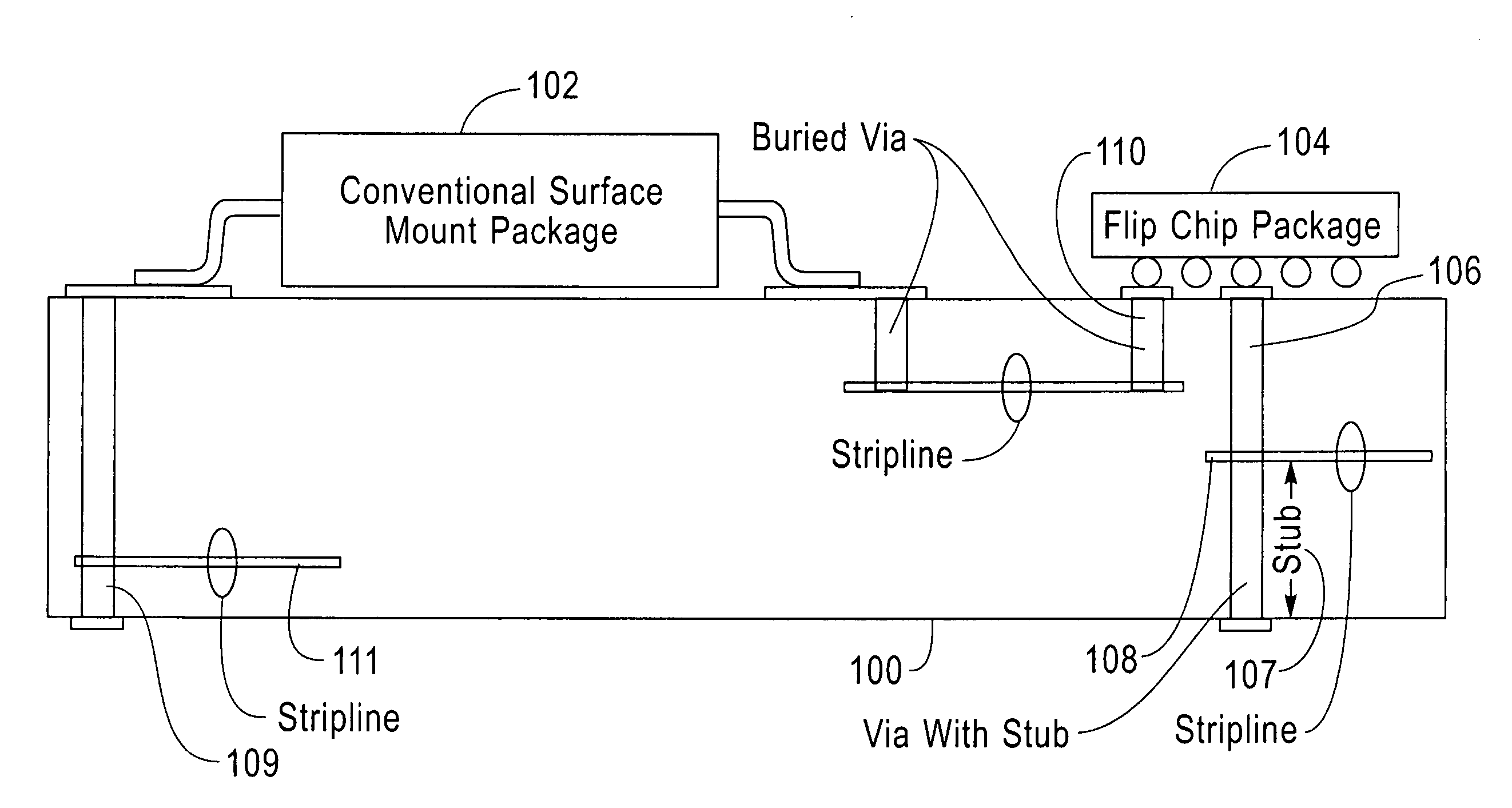
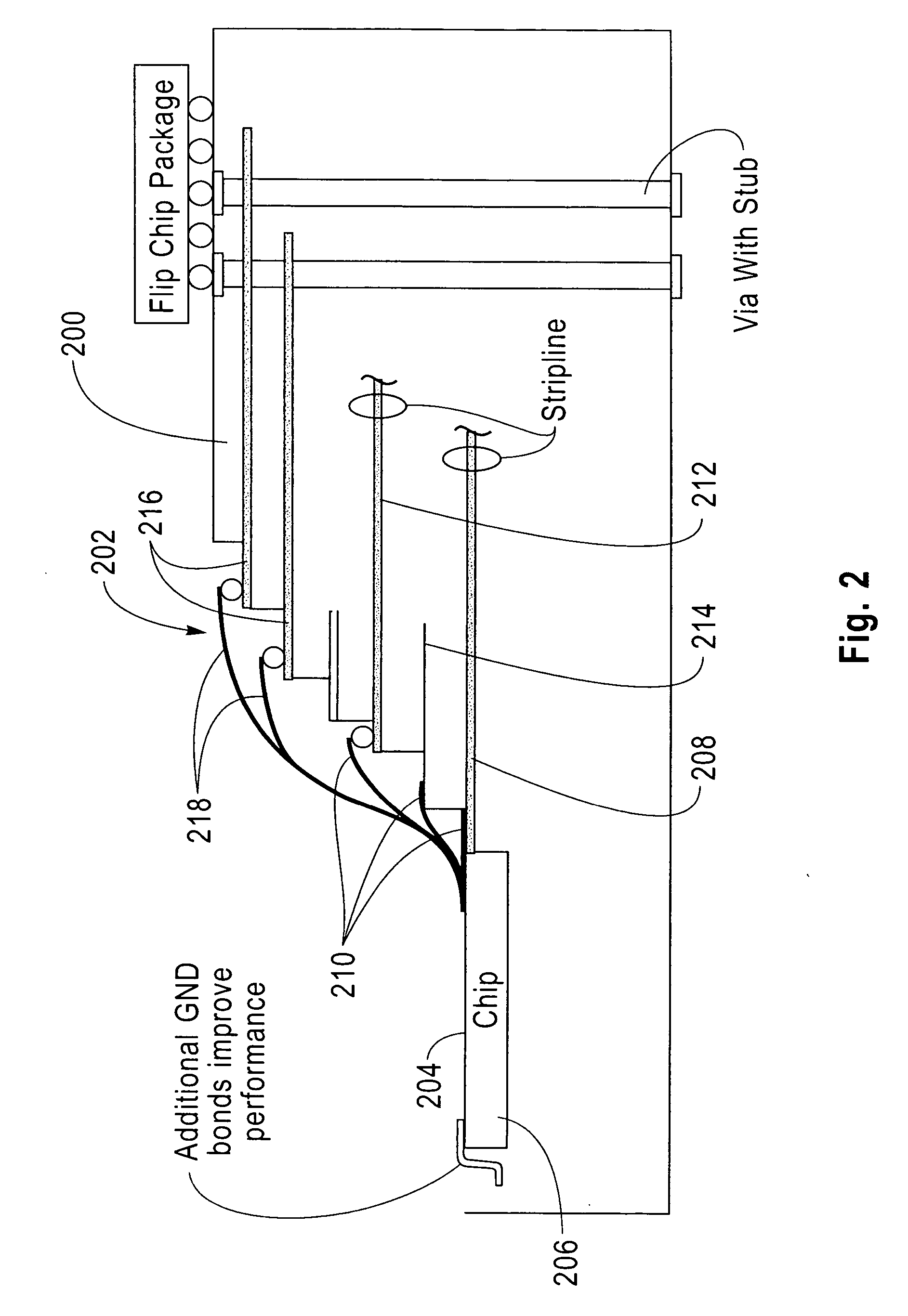
[0037] As explained above, there are many topologies conventionally available for implementing transmission lines in circuit boards (e.g., printed circuit boards (PCBs)). Internal embedded conductors, which may include an embedded conductor sandwiched between solid planes of a reference ground plane, offer many advantages over surface conductors. Embedded conductors support less dispersive transverse electric and magnetic modes which may be advantageous for wide band operation. An embedded conductor may also be self-shielding and, since they may undergo fewer processing steps than surface wiring they may be easier and less costly to fabricate.

[0038] Connecting an integrated circuit chip to embedded conductors conventionally requires the use of vias to connect from the surface of a printed circuit board where component...


PUM


Abstract

An electrical circuit device that includes a circuit board with an integrated circuit chip in a cavity that extends from a surface of the circuit board to an embedded conductor, and an electrical connection between the integrated circuit chip and the embedded conductor.

Description

[0001] This invention was made with Government support under Contract No: H98230-04-C-0920 awarded by the National Security Agency. The Government has certain rights in this invention.BACKGROUND OF THE INVENTION [0002] 1. Field of the Invention [0003] The present invention generally relates to integrated circuit chip packaging. More particularly, the present invention relates to integrated circuit chip packaging connecting an integrated circuit chip to a conductive layer embedded between layers of a printed circuit board. [0004] 2. Description of the Related Art [0005] Conventional methods and systems for connecting an integrated circuit chip to a printed circuit board have relied upon a surface attachment. A surface attachment restricts the launch to a conductive layer that is on the surface of a printed circuit board and if a signal from the integrated circuit chip must be launched into a conductive layer that is between the layers of the printed circuit board (i.e., an embedded c...

Claims


Application Information

Patent Timeline
Patent Type & Authority Applications(United States)
IPC IPC(8): G01R31/28
CPCH01L23/13H01L2224/16235H01L23/66H01L24/49H01L25/165H01L2223/6627H01L2224/16H01L2224/45014H01L2224/48091H01L2224/49109H01L2924/01027H01L2924/01029H01L2924/01047H01L2924/01078H01L2924/01079H01L2924/14H01L2924/1903H01L2924/3011H01L2924/3025H05K1/183H05K2201/092H05K2201/09845H05K2203/049H01L23/3677H01L2924/15192H01L2224/16225H01L24/73H01L24/48H01L2924/01006H01L2924/01033H01L2924/014H01L2924/00014H01L2224/45099H01L2224/05599H01L2924/206H01L2224/73221H05K2201/09036H05K2201/0919H01L23/3675H01L23/49827H01L21/481H01L21/4882H01L23/3672H01L23/49838H01L24/16H01L24/40H01L24/45H01L2224/40105H01L2224/40237H01L2224/48471H01L2224/48472H01L2224/49433H01L2924/15153H01L2924/19031
Inventor KWARK, YOUNG HOON
Owner IBM CORP
Why Eureka
Try Eureka