

Waveform input circuit, waveform observation unit and semiconductor test apparatus
- Summary
- Abstract
- Description
- Claims
- Application Information
AI Technical Summary
Benefits of technology
Problems solved by technology
Method used
Image

Examples
first embodiment
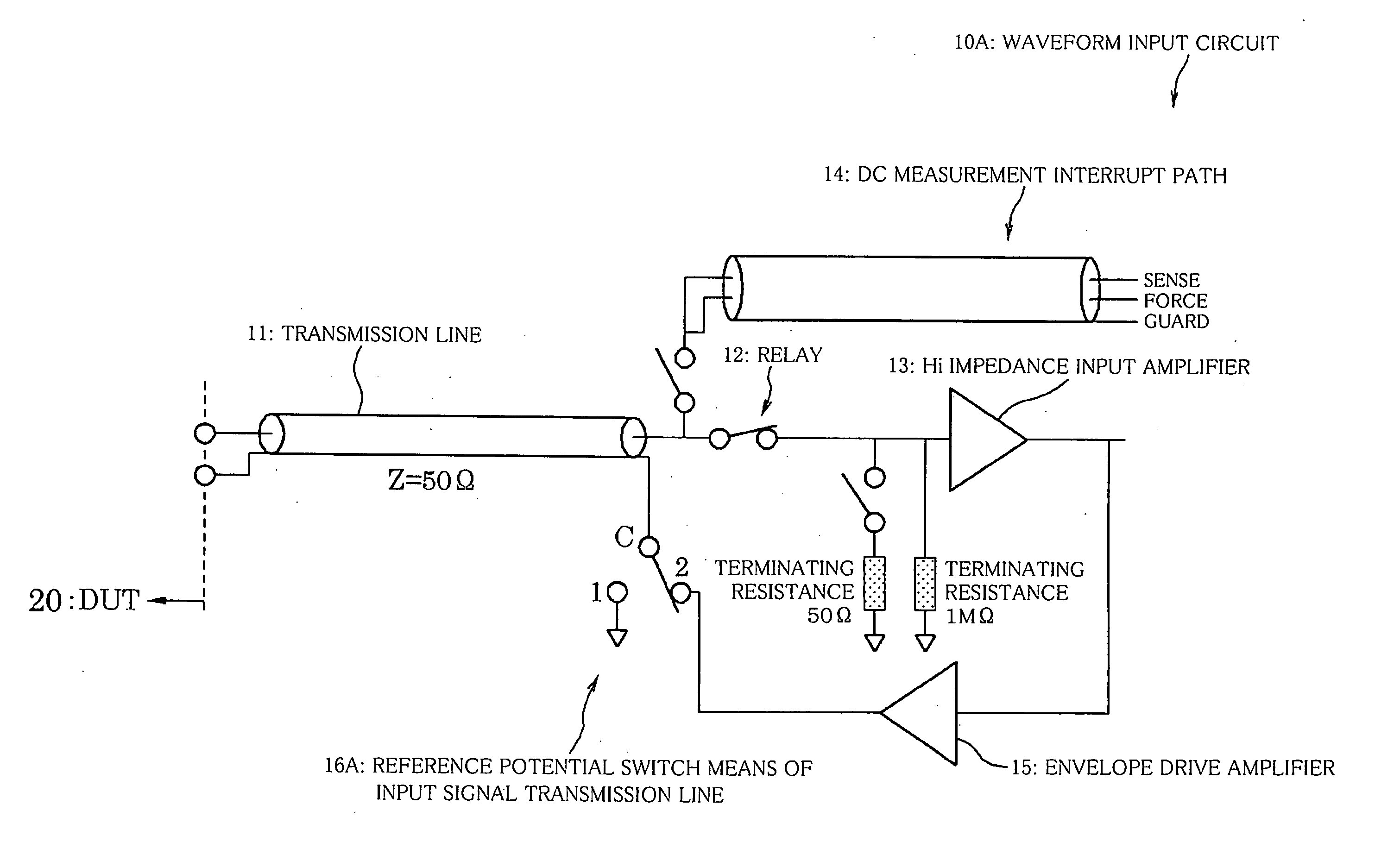
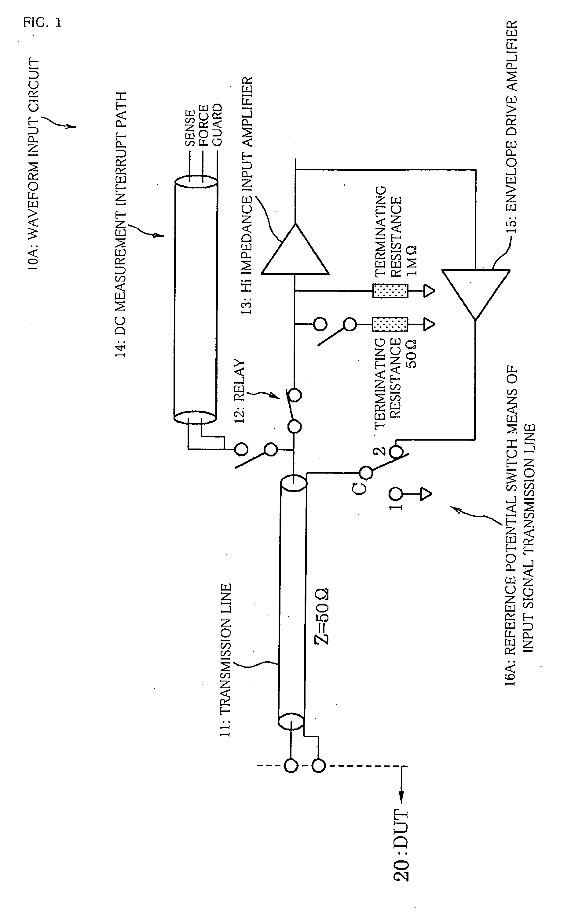
[0055] A first embodiment of a waveform input circuit of the present invention will first be described referring to FIG. 1.
[0056]FIG. 1 is a circuit configuration diagram showing the configuration of the waveform input circuit in the present embodiment.
[0057] It is to be noted that the waveform input circuit in the present embodiment is a circuit provided as an input section of a waveform observation unit. Further, the waveform observation unit is a test unit provided in a semiconductor test apparatus to observe an analog output waveform of a device under test.
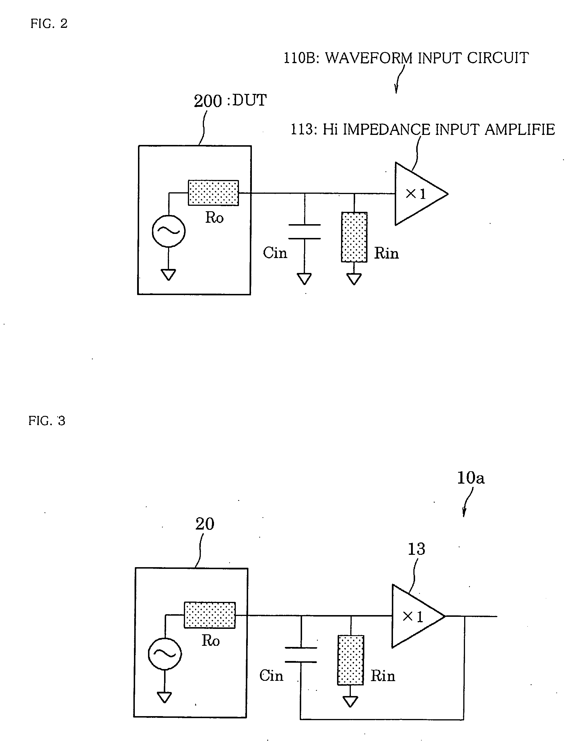
[0058] As shown in FIG. 1, a waveform input circuit 10a comprises a transmission line (input signal transmission line) 11 on which an output waveform from a device under test (DUT) 20 is transmitted, a terminating resistance 50 Ω, a terminating resistance 1 MΩ (Hi impedance), a relay (selection means) 12 which selects any one of the terminating resistances, a Hi impedance input amplifier (input buffer) 13, and a DC measurem...
second embodiment
[0070] Next, a second embodiment of a waveform input circuit of the present invention will be described with reference to FIGS. 5 and 6.
[0071]FIG. 5 shows the configuration of a conventional waveform input circuit comprising a plurality of transmission lines, and FIG. 6 shows the configuration of the waveform input circuit in the present embodiment.
[0072] The present embodiment is different from the first embodiment in that when a plurality of transmission lines is provided, the reference potential of one or two or more of the plurality of transmission lines can be switched by reference potential switch means of the input signal transmission lines. Other components are similar to those in the first embodiment.
[0073] Therefore, in FIG. 6, the same signs are assigned to the components similar to those in FIG. 1, and they will not be described in detail.
[0074] As shown in FIG. 5, a conventional waveform input circuit 110c; has a configuration in which there is provided a plurality ...
third embodiment
[0083] Next, a third embodiment of a waveform input circuit of the present invention will be described with reference to FIG. 7.
[0084]FIG. 7 is a circuit configuration diagram showing the configuration of the waveform input circuit in the present embodiment.
[0085] The present embodiment is different from the first embodiment in that reference potential switch means of the input signal transmission line can select a guard line of a DC measurement interrupt path. Other components are similar to those in the first embodiment.
[0086] Therefore, in FIG. 7, the same signs are assigned to the components similar to those in FIG. 1, and they will not be described in detail.
[0087] As shown in FIG. 7, a waveform input circuit 10c; of the present embodiment comprises a transmission line 11, a terminating resistance 50 Ω, a terminating resistance 1 MΩ, a relay 12, a Hi impedance input amplifier 13 and a DC measurement interrupt path 14, as well as an envelope drive amplifier 15 and reference ...
PUM
 Abstract
Description
Claims
Application Information