Probe Member for Wafer Inspection, Probe Card for Wafer Inspection and Wafer Inspection Apparatus

a technology for wafer inspection and probe cards, which is applied in the direction of measurement devices, semiconductor/solid-state device testing/measurement, instruments, etc., can solve the problems of difficult to produce the probe cards themselves, the pitch between the electrodes to be inspected in each integrated circuit is extremely small, and the price of the probe cards is extremely high. to achieve the effect of stable retention

Inactive Publication Date: 2007-11-22
JSR CORPORATIOON
View PDF7 Cites 6 Cited by
  • Summary
  • Abstract
  • Description
  • Claims
  • Application Information

AI Technical Summary

Benefits of technology

[0019] The present invention has been made on the basis of the foregoing circumstances and has as its object the provision of a probe member for wafer inspection, a probe card for wafer inspection and a wafer inspection apparatus, by which a good electrically connected state to a wafer, which is an object of inspection, can be su

Problems solved by technology

In order to produce a probe card used in such a probe test, it is however necessary to arrange a very great number of inspection probes, so that such a probe card is extremely expensive.
In addition, when the number of electrodes to be inspected is great, and the pitch thereof is fine, it is difficult to produce the probe card itself.
When a wafer that is an object of inspection is of a large size as at least 8 inches in diameter, and the number of electrodes to be inspected thereof is at least 5,000, particularly at least 10,000, however, a pitch between the electrodes to be inspected in each integrated circuit is extremely small so that the anisotropically conductive elastomer sheet in the above probe card involves the following problems.
However, it is extremely difficult to surely produce such an anisotropically conductive elastomer sheet because each conductive part is fine, and a proportion of the surface area of the conductive parts to the surface of the anisotropically conductive elastomer sheet is low though the area of the anisotropically conductive elastomer sheet is considerably large.
As a result, the production

Method used


Image

  • Probe Member for Wafer Inspection, Probe Card for Wafer Inspection and Wafer Inspection Apparatus
  • Probe Member for Wafer Inspection, Probe Card for Wafer Inspection and Wafer Inspection Apparatus
  • Probe Member for Wafer Inspection, Probe Card for Wafer Inspection and Wafer Inspection Apparatus

Examples


example 1

[Production of Sheet-Like Probe]

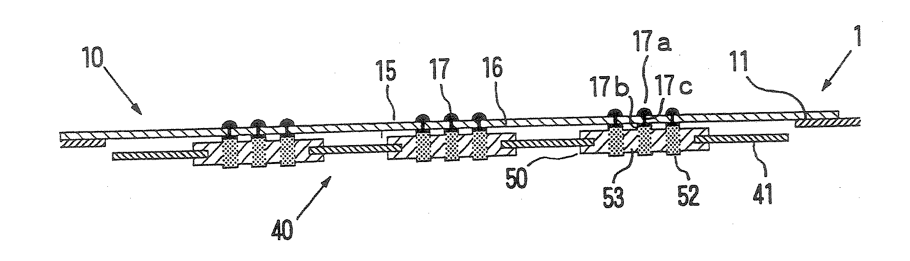
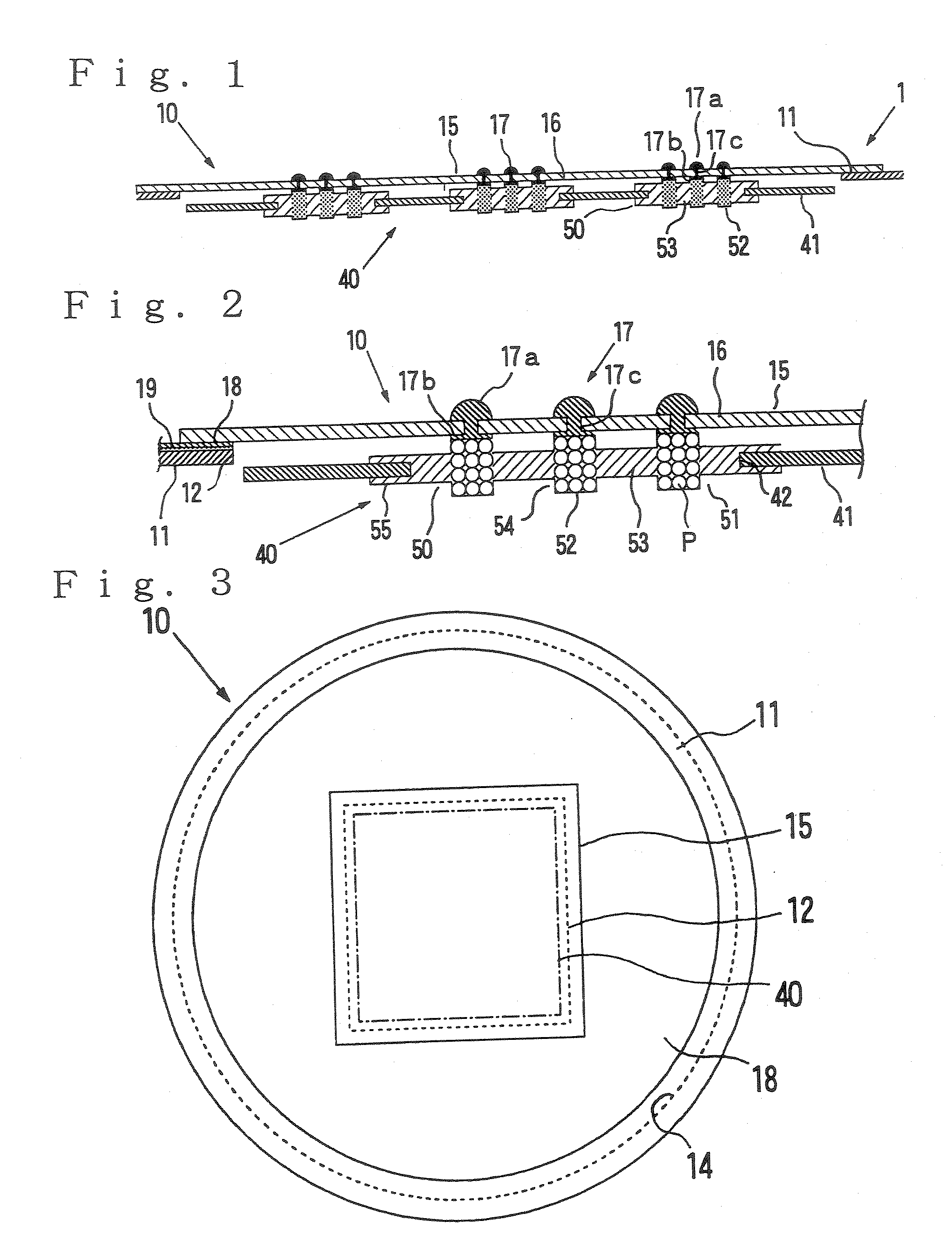
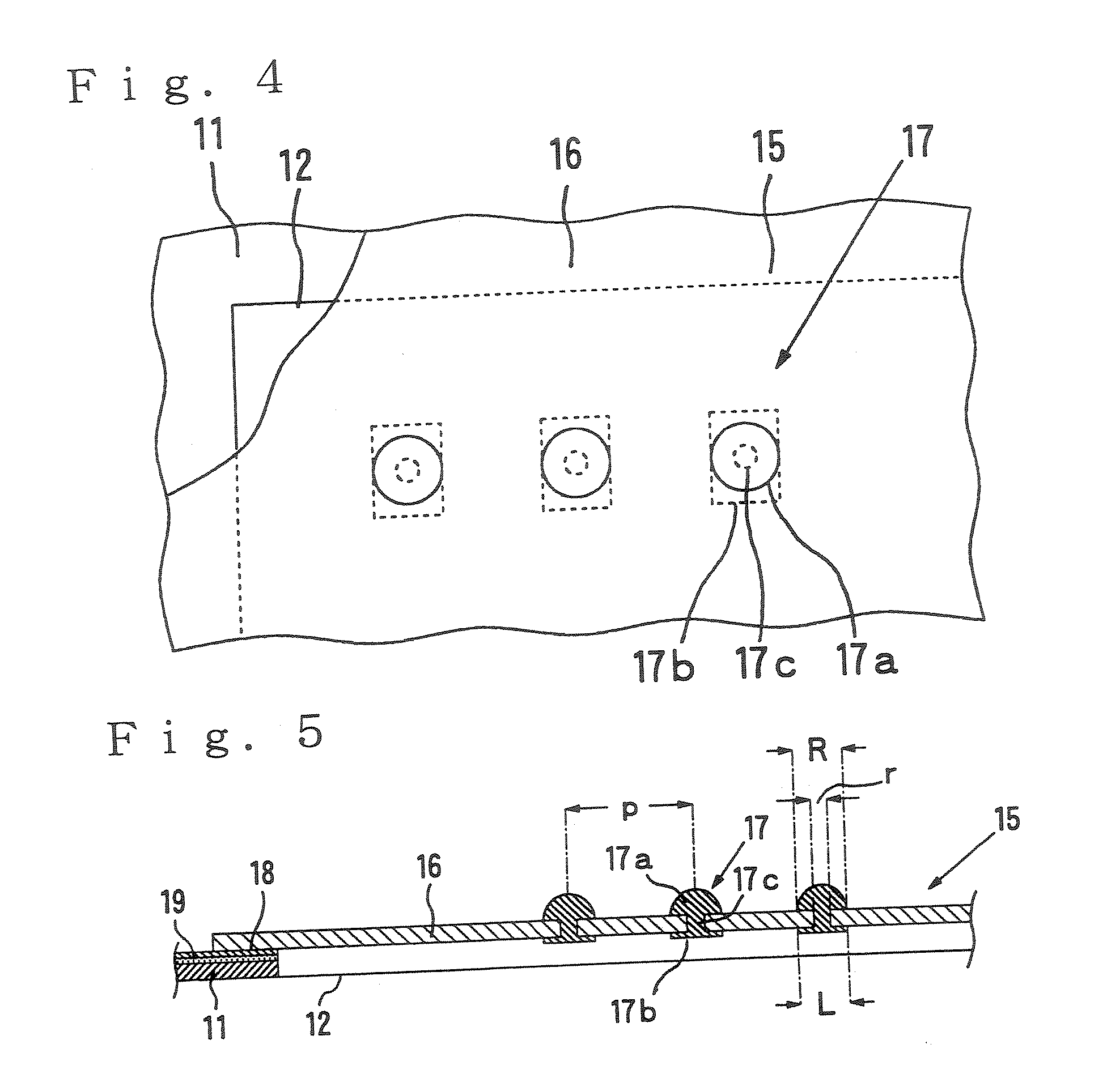
[0270] A frame plate (11) of the following specification was produced in accordance with the construction shown in FIG. 6.

[0271] This frame plate (11) is in a circular form having a diameter of 22 cm and a thickness of 100 μm, and has a rectangular opening (12) having dimensions of 90 mm×50 mm.

[0272] A laminate material (21B) obtained b integrally laminating a metal foil (22) for plating electrode and a metal foil (23) for forming holding parts, which each had a diameter of 20 cm and a thickness of 4 μm and were composed of copper, on both surfaces of a resin sheet (21A) for insulating protecting layer, which had a diameter of 20 cm and a thickness of 25 μm and was composed of polyimide, is provided (see FIG. 24).

[0273] A protecting film is formed on the whole front surface of the metal foil (22) for plating electrode by a protecting seal having a thickness of 25 μm and composed of polyethylene terephthalate, and a resist film, in which 1,280 circ...


PUM


Abstract

Provided are a probe member, a probe card and a wafer inspection apparatus, by which a good electrically connected state can be surely achieved, positional deviation by temperature change can be prevented, and the good electrically connected state can be stably retained even when a wafer has a diameter of 8 inches or greater, and the pitch of electrodes to be inspected is extremely small. The probe member of the invention has a sheet-like probe, which is composed of a frame plate made of a metal, in which an opening has been formed, and a plurality of contact films arranged on and supported by a front surface of the frame plate so as to close the opening, wherein the contact film is obtained by arranging, in a flexible insulating film, a plurality of electrode structures, and an anisotropically conductive connector, which is composed of a frame plate, in which a plurality of openings have been formed, and a plurality of elastic anisotropically conductive films arranged on and supported by the frame plate so as to close the respective openings, and is arranged on a back surface of the sheet-like probe. The opening of the frame plate in the sheet-like probe has a size capable of receiving the external shape in a plane direction in the frame plate of the anisotropically conductive connector.

Description

TECHNICAL FIELD [0001] The present invention relates to a probe member for wafer inspection, a probe card for wafer inspection and a wafer inspection apparatus, which are used for conducting electrical inspection of a plurality of integrated circuits formed on a wafer in a state of the wafer. BACKGROUND ART [0002] In the production process of semiconductor integrated circuit devices, after a great number of integrated circuits are formed on a wafer composed of, for example, silicon, a probe test that basic electrical properties of each of these integrated circuits are inspected, thereby sorting defective integrated circuits is generally conducted. This wafer is then diced, thereby forming semiconductor chips. Such semiconductor chips are housed and sealed in respective proper packages. Each of the packaged semiconductor integrated circuit devices is further subjected to a burn-in test that electrical properties thereof are inspected under a high-temperature environment, thereby sort...

Claims


Application Information

Patent Timeline
IPC IPC(8): G01R31/00
CPCG01R1/07307G01R1/073H01L22/00
Inventor YOSHIOKA, MUTSUHIKOFUJIYAMA, HITOSHIIGARASHI, HISAO
Owner JSR CORPORATIOON
Why Eureka
Try Eureka