Modulation methods and apparatus for reducing common mode noise

a technology of modulation methods and equipment, applied in pulse generators, pulse manipulation, pulse techniques, etc., can solve problems such as reducing system performance at a minimum, common mode current spikes, undesirable bearing currents, etc., and achieve the effect of reducing common mode nois

Active Publication Date: 2007-11-22
ROCKWELL AUTOMATION TECH
View PDF5 Cites 17 Cited by
  • Summary
  • Abstract
  • Description
  • Claims
  • Application Information

AI Technical Summary

Benefits of technology

[0020]At least some inventive embodiments include a method for reducing common mode noise in a three phase pulse width modulated (PWM) system that includes a three phase waveform generator that generates first, second and third initial modulating waveforms, a carrier signal generator that generates a carrier signal and a PWM generator that compares modulating waveforms and the carrier signal to generate duty cycle signals which are in turn used to generate switch control signals for controlling at least one of converter and inverter switches, the method comprising the steps of receiving the first, second and third initial modulating waveforms, identifying a first of the modulating waveforms that is instantaneously the maximum of the modulating waveforms, identifying a second of the modulating waveforms that is instantaneously the minimum of the modulating waveforms, for a first phase associated with at least one of the first and second identified waveforms, substituting a first substitute waveform for the one of the first and second waveforms, for the first phase, modifying at least one of the first substituted waveform and duty cycle signals generated by comparing the first substituted waveform with the carrier signal as a function of a first rule set to substantially minimize the effects of turn on delays and for at least one of the second and third phases, modifying at least one of the associated modulating waveform and duty cycle signals generated by comparing the modulating waveform with the carrier signal as a function of a second rule set to substantially eliminate the effects of turn on delays where the second rule set is different than the first rule set.
[0025]Some embodiments further include the steps of, for the second phase that is associated with the second identified waveform, substituting a second substitute waveform for the second waveform, modifying at least one of the second substituted waveform and duty cycle signals generated by comparing the second substituted waveform with the carrier signal as a function of the first rule set to substantially minimize the effects of turn on delays. In some cases the step of substituting the first substitute waveform includes substituting the second identified waveform for the first identified waveform and wherein the step of substituting the second substitute waveform includes substituting the first identified waveform for the second identified waveform. In some cases the modifying steps include modifying the modulating waveforms, the method further including the steps of identifying the direction of carrier signal count and identifying the polarities of the currents in each of the three phases, the first and second rule sets causing modification of the waveforms as a function of the direction of carrier signal count and the phase current polarity.
[0027]Some embodiments include a method for reducing common mode noise in a three phase pulse width modulated (PWM) system that includes a three phase waveform generator that generates first, second and third modulating waveforms, a carrier signal generator that generates a carrier signal and a PWM generator that compares modulating waveforms and the carrier signal to generate switch control signals for controlling at least one of converter and inverter switches, the method comprising the steps of receiving the modulating waveforms, identifying the direction of carrier signal count, identifying the polarities of the three phase currents, for a first of the modulating waveforms, substituting a second of the modulating waveforms where the first modulating waveform is associated with a first phase, when the first phase current is positive and the carrier direction is up, subtracting a compensation voltage from the substituted modulating waveform to generate a first compensated modulating waveform, when the first phase current is negative and the carrier direction is down, adding the compensation voltage to the substituted modulating waveform to generate the first compensated modulating waveform, when the third phase current is negative and the carrier direction is up, subtracting a compensation voltage from the modulating waveform associated with the third phase and, when the third phase current is positive and the carrier direction is down, adding the compensation voltage to the modulating waveform associated with the third phase thereby generating another compensated modulating waveform and using the compensated modulating waveforms to generate switch control signals for controlling the one of the inverter and the converter.

Problems solved by technology

CMV pulses cause CMV dv / dts which in turn cause common mode current (CMC) spikes.
CMV and associated CMC have been known to reach levels beyond motor winding insulation ratings and can result in undesirable bearing currents.
Consequently, CMV and CMC often reduce system performance at a minimum and have been known to damage motor components.
Unfortunately synchronization of the switching sequences is not easy to facilitate when the switching frequency of the boost rectifier is different than the frequency of the inverter.
Unfortunately, this vector shifting SVPWM control scheme cannot be applied to diode rectifier / inverter systems.
Calculating dwell times in real time requires excessive dedicated computing power.

Method used


Image

  • Modulation methods and apparatus for reducing common mode noise
  • Modulation methods and apparatus for reducing common mode noise
  • Modulation methods and apparatus for reducing common mode noise

Examples


Embodiment Construction

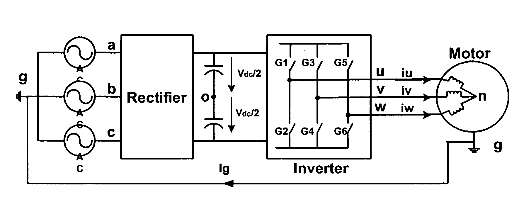
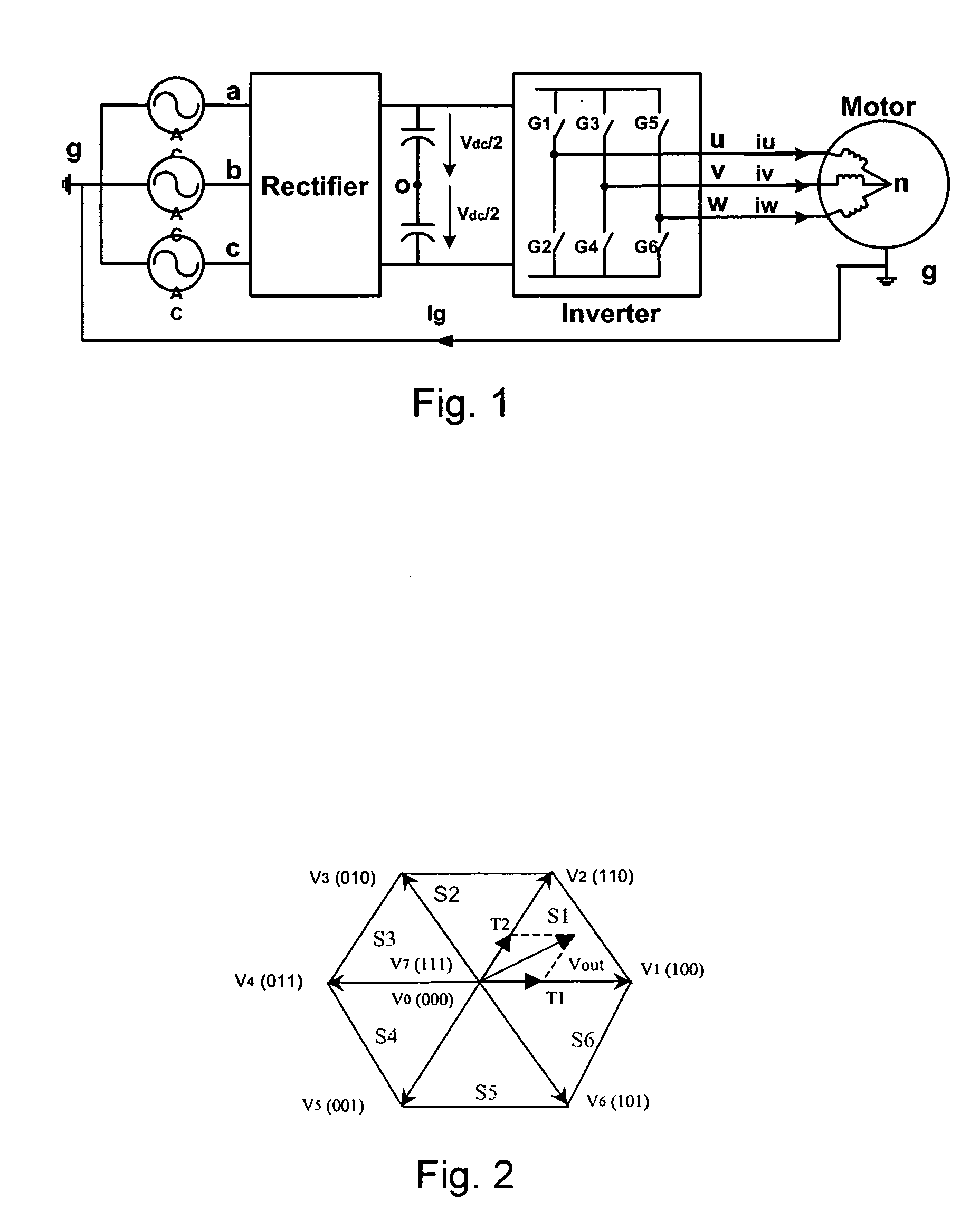
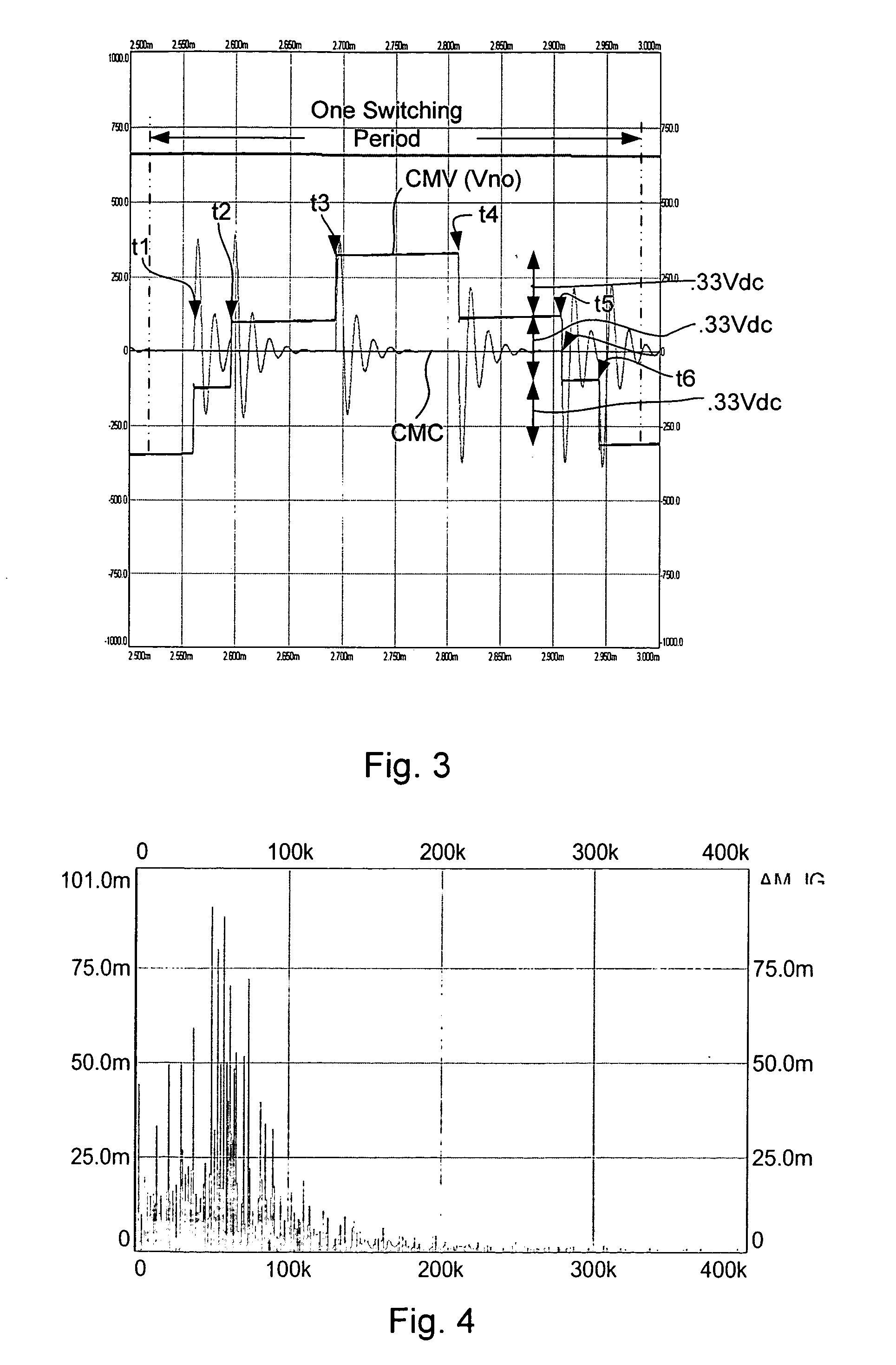
[0074]The common mode noise reduction schemes described herein are to be used with carrier-based PWM control systems and do not require dwell-time calculations. The schemes can be applied to active rectifiers as well as PWM inverters to reduce common mode noise which includes both CMV and CMC.

[0075]Herein three different schemes are disclosed that each have substantially identical results and that are to be employed under different circumstances. To this end, it has been recognized that some drives are programmable off the shelf to generate switch trigger patterns or control signals required to reduce common mode noise completely in software while others require additional hardware. The first scheme described herein is implemented completely in software that is run on an off the shelf drive, the second scheme is implemented in part in software run by a standard drive and in part by additional hardware and the third scheme is implemented in hardware that is added to a standard drive....


PUM


Abstract

A method and apparatus for reducing common mode noise in a three phase pulse width modulated (PWM) system the method comprising the steps of receiving modulating waveforms, identifying a first of the modulating waveforms that is instantaneously the maximum of the modulating waveforms, identifying a second of the modulating waveforms that is instantaneously the minimum of the modulating waveforms, for a first phase associated with at least one of the first and second identified waveforms, substituting a first substitute waveform for the one of the first and second waveforms, for the first phase, modifying at least one of the first substituted waveform and duty cycle signals generated by comparing the first substituted waveform with the carrier signal as a function of a first rule set to substantially minimize the effects of turn on delays and for at least one of the second and third phases, modifying at least one of the associated modulating waveform and duty cycle signals generated by comparing the modulating waveform with the carrier signal as a function of a second rule set to substantially eliminate the effects of turn on delays where the second rule set is different than the first rule set.

Description

CROSS-REFERENCE TO RELATED APPLICATIONS[0001]Not applicable.STATEMENT REGARDING FEDERALLY SPONSORED RESEARCH OR DEVELOPMENT[0002]Not applicable.BACKGROUND OF THE INVENTION[0003]The present invention relates generally to methodologies for reducing the common mode noises generated by two-level rectifier / inverter variable frequency drive (VFD) systems. This invention more particularly relates to modulation techniques for common mode noise reduction.[0004]Referring to FIG. 1, an exemplary two-level rectifier / inverter variable frequency drive (VFD) system is shown that includes a three phase voltage source, a rectifier, a three phase inverter and a load (e.g., a motor). The rectifier may be either a diode type (i.e., constructed using diodes) or an active type (i.e., a boost type including controllable switching devices that is controlled via pulse width modulation (PWM) or the like). Where the rectifier is active, the rectifier typically includes six switching devices (e.g., solid state...

Claims


Application Information

Patent Timeline
Patent Type & Authority Applications(United States)
IPC IPC(8): H03K3/017
CPCH02P27/08H02M2001/123H02M7/5395H02M1/12H02M1/123
Inventor YIN, QIANGKERKMAN, RUSSEL J.
Owner ROCKWELL AUTOMATION TECH
Why Eureka
Try Eureka