Integrated circuit package having exposed thermally conducting body

a technology of integrated circuits and thermal conductors, applied in semiconductor devices, semiconductor/solid-state device details, electrical apparatus, etc., can solve the problems of poor thermal performance and high package profile, and achieve the effects of improving thermal, electrical and mechanical performance, reducing profile size, and improving reliability of package board mounts

Inactive Publication Date: 2007-11-29
AVAGO TECH WIRELESS IP SINGAPORE PTE
View PDF59 Cites 43 Cited by
  • Summary
  • Abstract
  • Description
  • Claims
  • Application Information

AI Technical Summary

Benefits of technology

[0012]Apparatuses, methods, and systems for improved integrated circuit packages are described. Embodiments of the present invention provide improved thermal, electrical, and

Problems solved by technology

Conventional BGA packages, such as shown in FIG. 1, have drawbacks, including: (1) a high package profile; (2) poor thermal perf

Method used


Image

  • Integrated circuit package having exposed thermally conducting body
  • Integrated circuit package having exposed thermally conducting body
  • Integrated circuit package having exposed thermally conducting body

Examples


example advantages

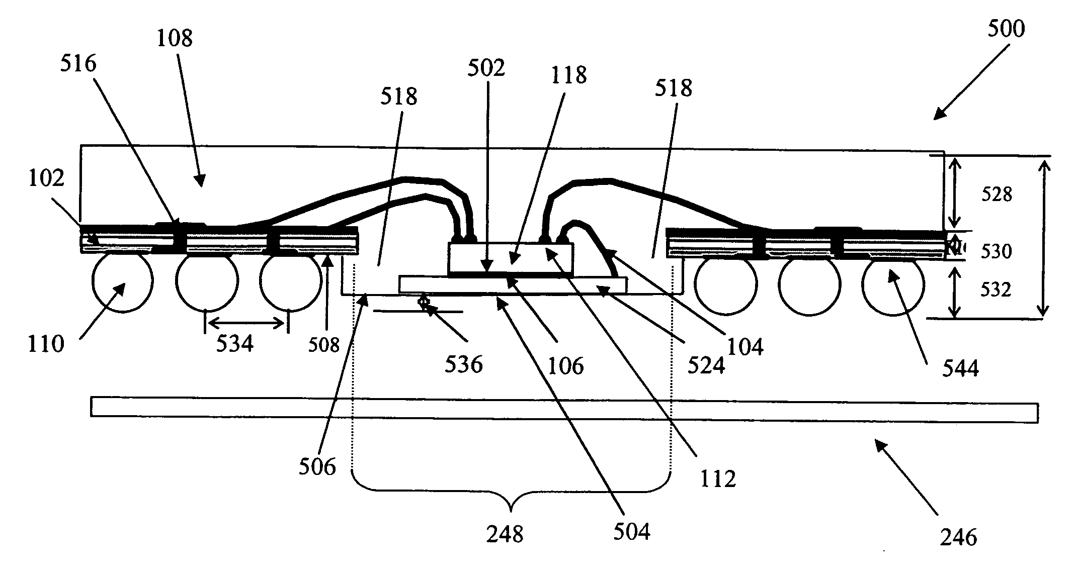
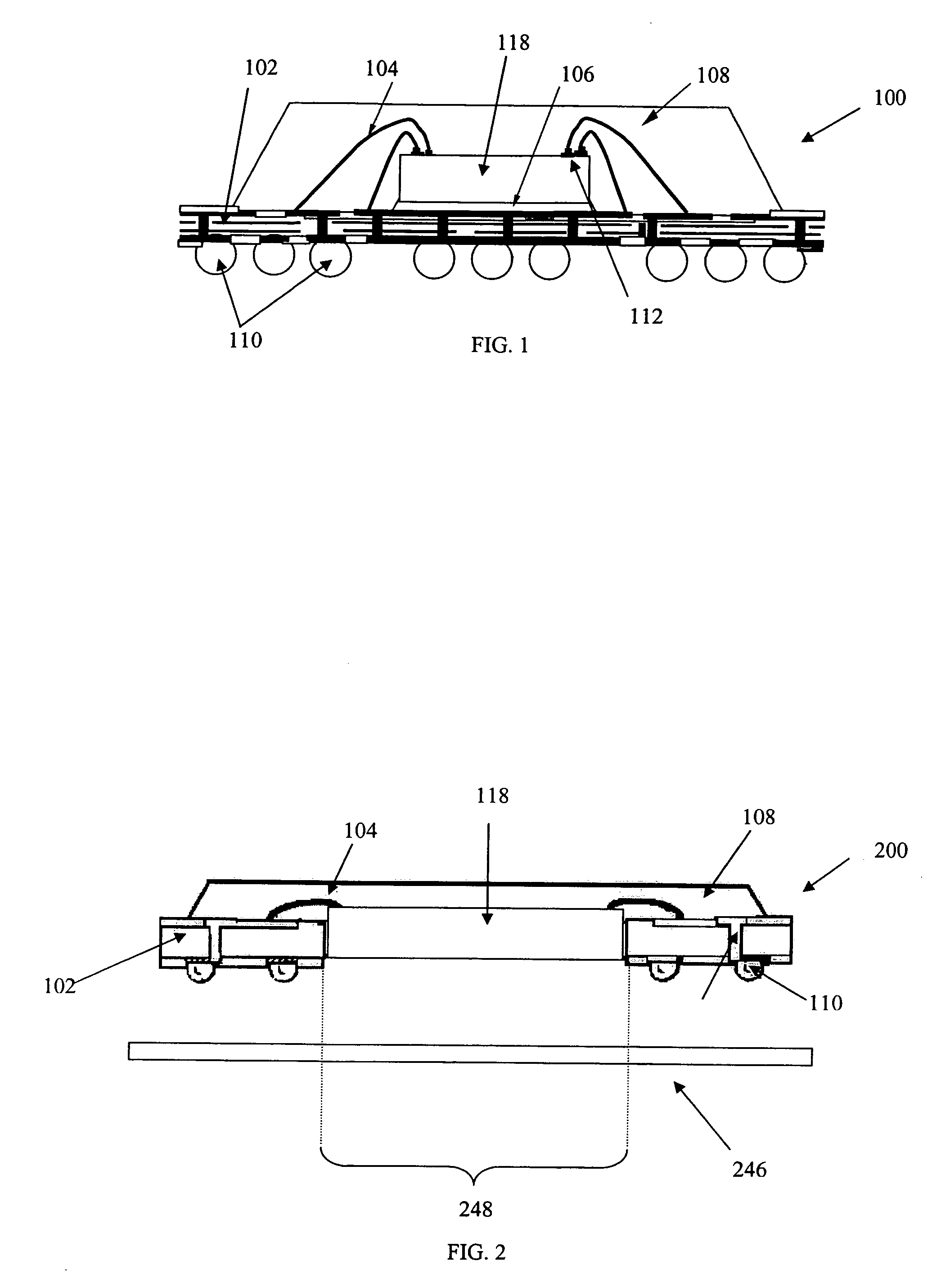
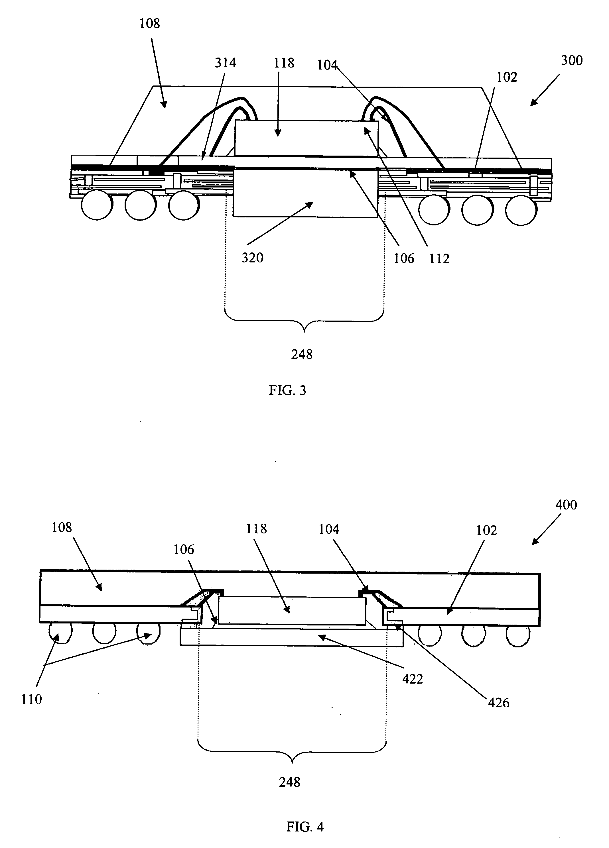
[0098]Embodiments of the present invention provide many advantages over conventional BGA packages, including those described above with respect to FIGS. 1-4. Some of these advantages are described below. Each advantage described below does not necessarily apply to each embodiment described herein. Furthermore, the advantages provided by embodiments of the present invention are not necessarily limited to those described below.

[0099](1) Placing the IC die in an opening in the substrate and reducing the length of wirebonds necessary to connect the IC die to the substrate substantially reduces the height of the package profile and increases reliability of the package as a whole.

[0100](2) The die attach step used in a conventional die-up BGA package assembly process is not needed. Because of this, potential reliability issues associated with the die attach interface for conventional IC packages, such as both BGA and leadframe types, are removed. For example, an undesirable “popcorn pheno...


PUM


Abstract

An apparatus and method for a wire-bond die-up area array package is described. The package includes an integrated circuit (IC) die, a substrate, and a thermally conducting body. A bottom surface of the IC die is exposed through an opening in a central region of the substrate. The die is mounted to the thermally conducting body. A bottom surface of the thermally conducting body is configured to be connected to a circuit board, such as a PWB, when the package is mounted to the circuit board. The bottom surface of the thermally conducting body may be connected directly to the circuit board, or may be coupled to the circuit board via solder balls or other mechanism. One or more wirebonds are used to electrically connect the die to a top surface of the substrate. A mold compound encapsulates the die, the wirebonds, and at least a portion of the top surface of the substrate, and fills a gap between peripheral edges of the IC die and inner walls of the substrate central window opening. A matrix of solder balls is attached to a bottom surface of the substrate.

Description

[0001]This application claims the benefit of U.S. Provisional Appl. No. 60 / 808,543, filed May 26, 2006, which is incorporated by reference herein in its entirety.BACKGROUND OF THE INVENTION[0002]1. Field of the Invention[0003]The embodiments of the present invention relate to integrated circuit (IC) device packaging technology, and in particular, to ball grid array (BGA) packages having improved thermal and / or electrical characteristics.[0004]2. Related Art[0005]The die-up plastic ball grid array package was first introduced by Motorola and was called Overmolded Plastic Pad Array Carriers (OMPAC). For further detail on this package, refer to “Overmolded Plastic Pad Array Carriers (OMPAC): A Low Cost, High Interconnect Density IC Packaging Solution for Consumer and Industrial Electronics,” Electronic Components and Technology Conference, IEEE, pp. 176-182, 1991, which is incorporated by reference herein in its entirety. Commonly known as a “PBGA” package, the plastic ball grid array ...

Claims


Application Information

Patent Timeline
IPC IPC(8): H01L23/34
CPCH01L23/13H01L2224/16145H01L23/4334H01L24/33H01L2224/32225H01L2224/48091H01L2224/48227H01L2224/48237H01L2224/48465H01L2224/73265H01L2224/85001H01L2224/92H01L2224/92247H01L2924/01013H01L2924/01029H01L2924/01047H01L2924/0105H01L2924/01079H01L2924/09701H01L2924/15311H01L2924/30107H01L2924/3011H01L23/3128H01L2224/48247H01L24/48H01L2924/01005H01L2924/01006H01L2924/01033H01L2924/01074H01L2224/32245H01L2224/16225H01L2924/00014H01L2924/00H01L2924/00012H01L2924/3512H01L24/73H01L2224/32145H01L2924/14H01L2924/15153H01L2924/15787H01L2924/181H01L2924/18165H01L2924/351H01L2224/45099H01L2224/45015H01L2924/207
Inventor ZHAO, SAM ZIQUNLAW, EDWARDKHAN, REZAUR RAHMAN
Owner AVAGO TECH WIRELESS IP SINGAPORE PTE
Why Eureka
Try Eureka