

Organic light-emitting display device
- Summary
- Abstract
- Description
- Claims
- Application Information
AI Technical Summary
Benefits of technology
Problems solved by technology
Method used
Image

Examples
first embodiment
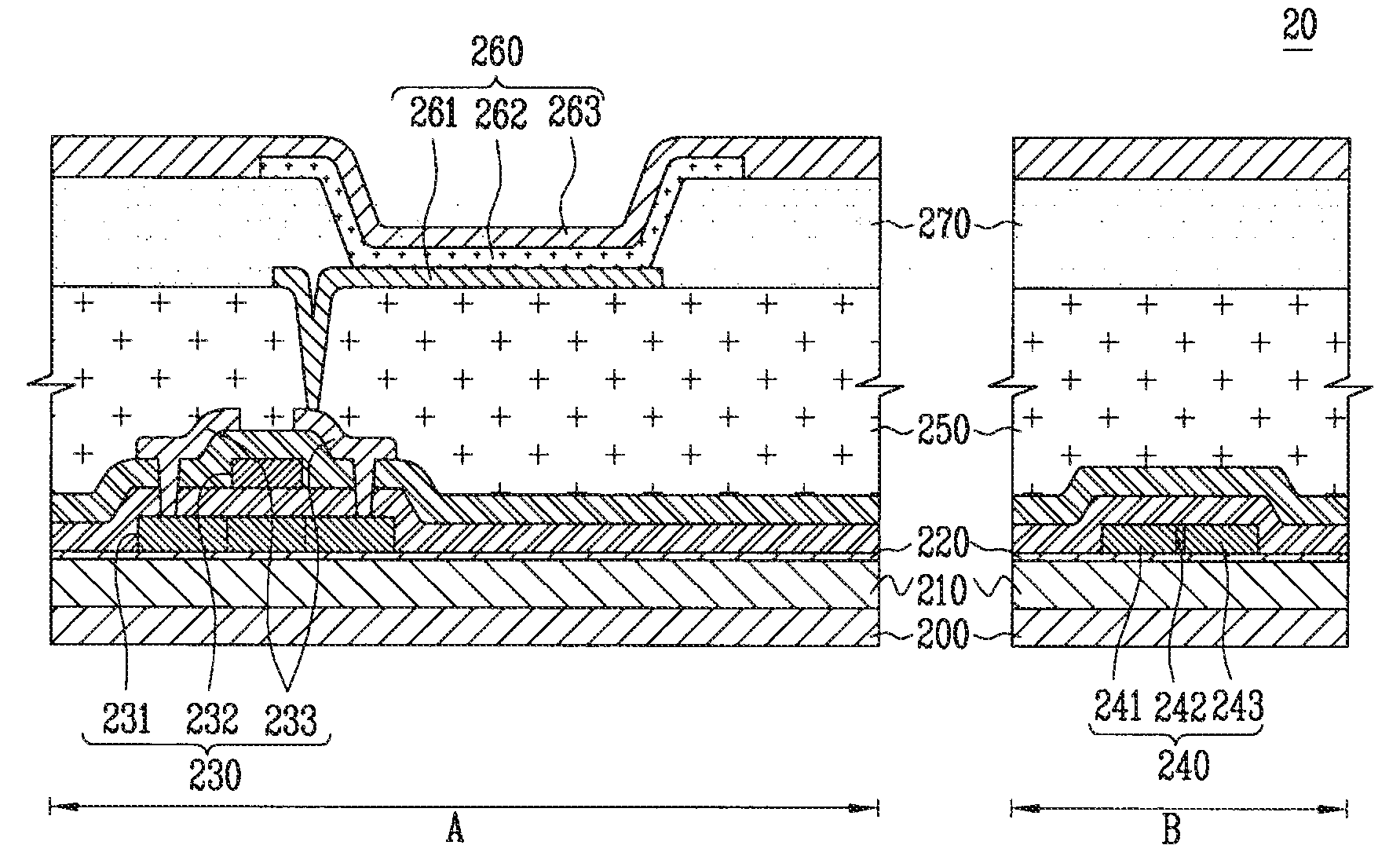
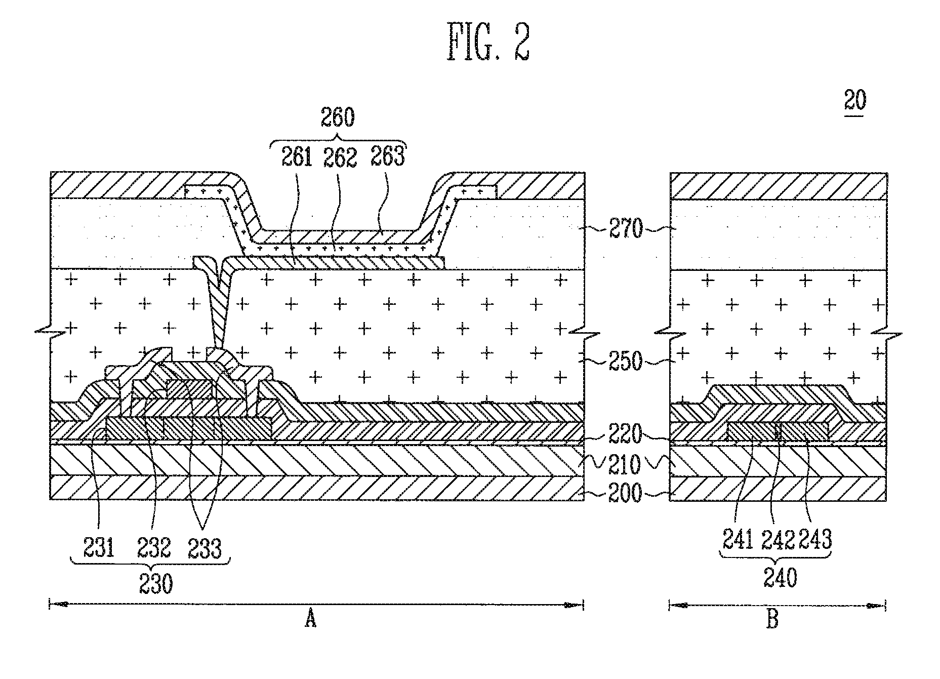
[0026]FIG. 2 is a cross-sectional view of an organic light emitting diode having a photo diode according to the present invention.
[0027]Referring to FIG. 2, an organic light emitting diode 20 according to the present invention includes: a substrate 200 having a pixel region A and a non-pixel region B; a first buffer layer 210 and a second buffer layer 220 formed over the substrate 200; a thin film transistor 230 formed over the second buffer layer 220; an organic light emitting device 260 formed in the pixel region A of the substrate 200 and electrically connected with the thin film transistor 230; and a photo diode 240 formed in the non-pixel region B and for receiving external light of red wavelength at a certain or predetermined absorption rate, wherein the first buffer layer 210 is formed to be from 2900 Å to 3100 Å in thickness, the second buffer layer 220 is formed to be from 200 Å to 400 Å in thickness, and the photo diode 240 includes an N-type doping region 241, a channel r...
second embodiment
[0048]FIG. 4 is a cross-sectional view of an organic light emitting diode having a photo diode according to the present invention. For the convenience of explanation, elements that are substantially the same as those in the aforementioned FIG. 2 will not be described again. In particular, the description on the substrate on which the thin film transistor is formed will not be described again.
[0049]In FIG. 4, a first buffer layer 310 and a second buffer layer 320 are formed over a substrate 300. The first buffer layer 310 is made of a silicon oxide film SiO2 and is formed to be from 700 Å to 900 Å in thickness, and, in one embodiment, it is formed to be 800 Å in thickness. The second buffer layer 320 is made of a silicon nitride film SiNx and is formed to be from 100 Å to 300 Å in thickness, and, in one embodiment, it is formed to be 200 Å in thickness. The thickness of the first buffer layer 310 and the thickness of the second buffer layer 320 are formed to have the above thickness ...
third embodiment
[0062]FIG. 6 is a cross-sectional view of an organic light emitting diode having a photo diode according to the present invention. For the convenience of explanation, elements that are substantially the same as those in the aforementioned FIG. 2 will not be described again. In particular, the description on the substrate on which the thin film transistor is formed will not be described again.
[0063]In FIG. 6, a first buffer layer 410 and a second buffer layer 420 are formed over a substrate 400. The first buffer layer 410 is made of a silicon oxide film SiO2 and is formed to be from 700 Å to 900 Å in thickness, and, in one embodiment, it is formed to be 800 Å in thickness. The second buffer layer 420 is made of a silicon nitride film SiNx and is formed to be from 300 Å to 500 Å in thickness, and, in one embodiment, it is formed to be 400 Å in thickness. The thickness of the first buffer layer 410 and the thickness of the second buffer layer 420 are formed to have the above thickness ...
PUM
 Abstract
Description
Claims
Application Information