Solid state image wavelength converter

a wavelength converter and solid-state technology, applied in the field of solid-state wavelength converters, can solve the problems of reducing the spatial resolution reducing the sensitivity of the wavelength converter, and the presence of the mirror tending to increase the distance, so as to achieve the effect of improving sensitivity

Inactive Publication Date: 2007-11-29
MICROSOFT INT HLDG BV
View PDF12 Cites 7 Cited by
  • Summary
  • Abstract
  • Description
  • Claims
  • Application Information

AI Technical Summary

Benefits of technology

[0012] An aspect of the invention relates to providing a solid state wavelength converter having improved sensitivity so that output light from the wavelength converter is useable to provide relatively high-resolution images of an object when intensity of input light from the object is relatively low.
[0014] Electrons from electron-hole pairs, generated in the photo-conducting layer by input light incident on the converter from an object being imaged, drift through the multiplication region on their way to the photo-modulation layer. The drifting electrons ionize material in the multiplication region and multiply in an avalanche process. As a result, the number of electrons that reach the photo-modulation layer is substantially increased over the number that would reach the photo-modulation layer in the absence of the multiplication region. The sensitivity of the wavelength converter is therefore substantially increased over that of prior art wavelength converters.
[0015] An aspect of some preferred embodiments of the present invention relates to providing a wavelength converter in which input light photons have lower energy than output light photons and the output light passes through both the photo-conducting and photo-modulation layers of the converter. Such a wavelength converter can, for example, convert an IR input image of an object into a visible image of the object without the need to provide a mirror between the photo-conducting layer and the photo-modulation layer. As a result, the resolution of the visible image is not degraded by distortions, described above, that a mirror causes in a modulation field generated in the wavelength converter responsive to the IR input image.
[0017] An aspect of some preferred embodiments of the present invention relates to preventing electrons formed in the photo-conducting layer by passage of output light through the photo-conducting layer from destroying correlation between modulation of output light and an input image of an object that is encoded in input light.
[0021] In order to prevent the lack of correspondence between the modulation field and the input image from affecting modulation of the output light, in accordance with a preferred embodiment of the present invention, output light that illuminates the converter is provided in the form of short pulses of light. The pulse width of a pulse of output light is so short that the pulse substantially completely traverses the photo-modulation layer of the converter before electrons generated by the pulse in the photo-conducting layer reach the photo-modulation layer and affect a modulation field in the photo-modulation layer. Therefore, when a charge image is generated in the wavelength converter by input light from an object, output light that subsequently illuminates the converter is substantially accurately modulated in accordance with the charge image. Modulation of the output light pulse is substantially unaffected by passage of the output light pulse through the wavelength converter even though, in passing through the photo-conducting layer, the output light pulse produces electron-hole pairs in the photo-conducting layer.
[0024] In some preferred embodiments of the present invention, in which the photo-modulation layer is a positive image modulator, the output light passes through the photo-modulation layer before it passes through the photo-conducting layer. In these preferred embodiments of the present invention, an electron density in the photo-conducting layer that is generated from electron-hole pairs produced by the passage of output light through the photo-modulation layer is homologous with the input image. Electrons from this electron density that drift to the photo-modulation layer do not destroy correspondence between the input image and a modulation field in the photo-modulation layer. Instead, the electrons amplify the modulation field while maintaining the correspondence between the modulation field and the input image.

Problems solved by technology

However, in wavelength converters with a mirror, the presence of the mirror tends to increase the distance between a charge image formed in the wavelength converter and the wavelength converter's photo-modulation layer.
Therefore, the mirror tends to reduce the spatial resolution of the wavelength converter.
In many prior art wavelength converters, for practical intensities of input light, variations in the density of trapped electrons are often too small to affect acceptable modulation of output light.
As a result, the sensitivity of these wavelength converters is not sufficient for many applications.

Method used


Image

  • Solid state image wavelength converter
  • Solid state image wavelength converter
  • Solid state image wavelength converter

Examples


Embodiment Construction

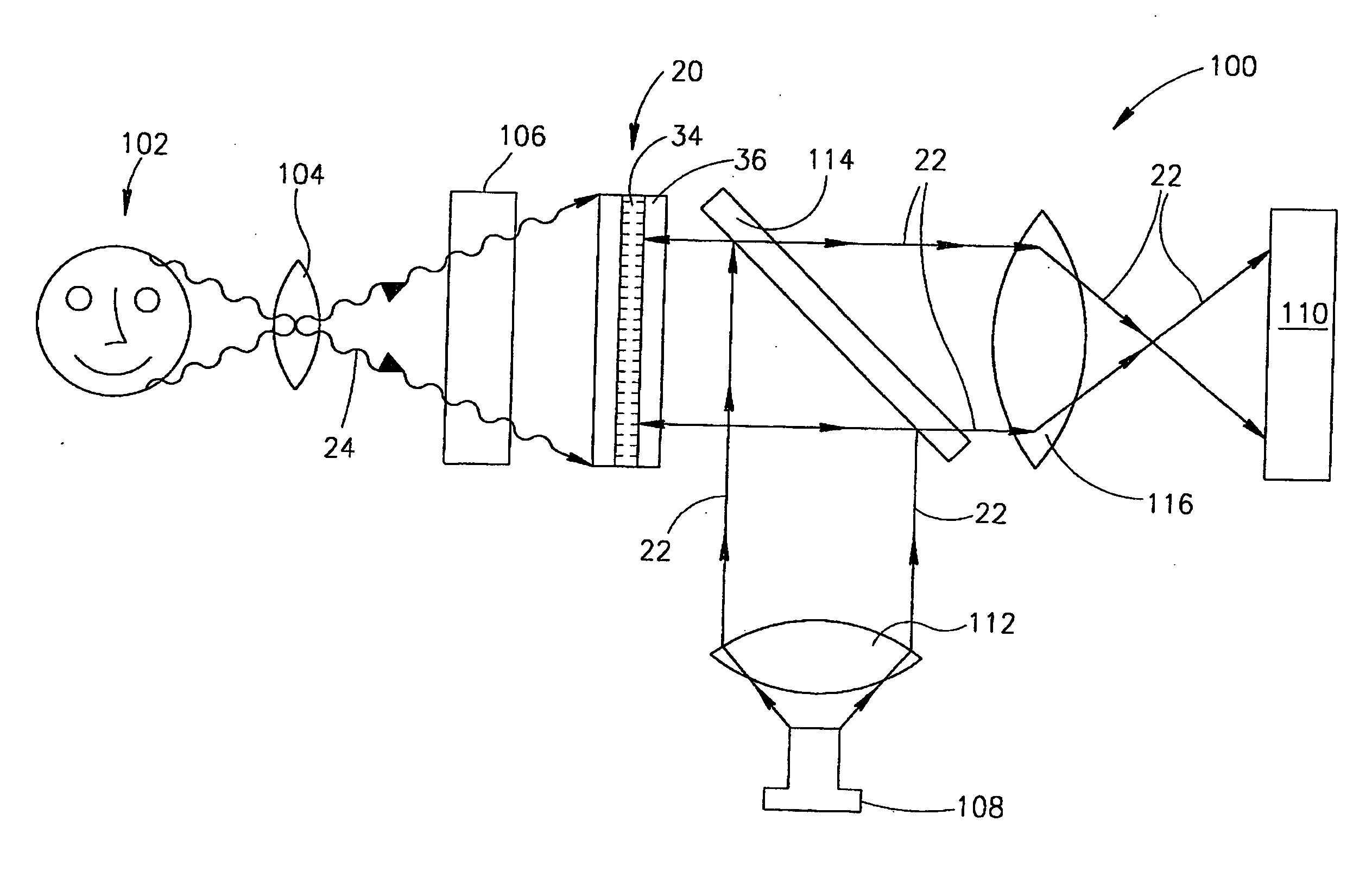
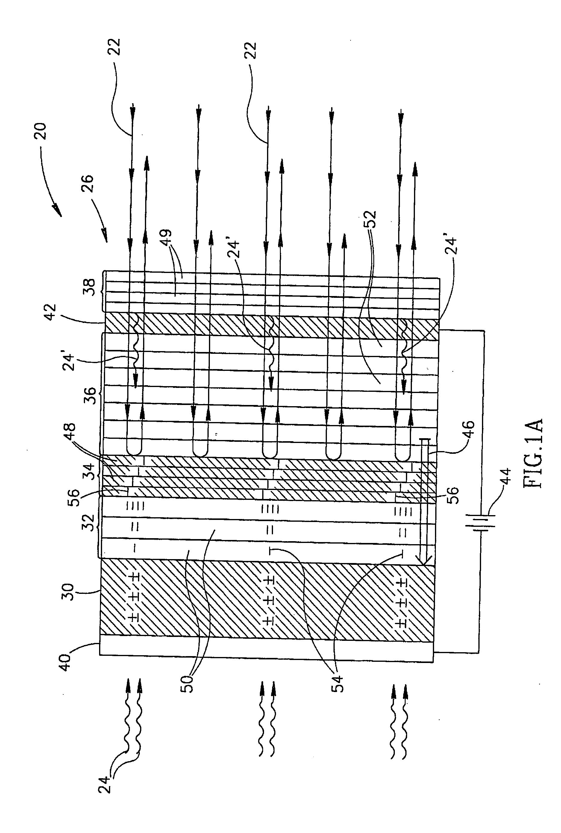
[0077]FIG. 1A schematically shows a cross section view of a solid state wavelength converter 20 encoding output light, represented by straight line arrows 22, with an image encoded in input light, represented by wavy arrows 24, in accordance with a preferred embodiment of the present invention. Input light 24 has a spatially varying intensity represented schematically by the clustering of wavy arrows 24 into groups. The varying intensity encodes an image of an object.

[0078] Wavelength converter 20 preferably comprises a layered body 26 comprising a heavily p doped layer 40, a photo-conducting layer 30, an electron multiplication region 32, a first dielectric mirror 34, a photo-modulation region 36, a heavily n-doped layer 42 and a second dielectric mirror 38. A power supply 44 back biases the p and n doped conducting layers 40 and 42 and generates an electric field, represented by and having a direction indicated by double arrow 46, in the layers sandwiched between them. Electric f...


PUM

PropertyMeasurementUnit
wavelengthaaaaaaaaaa
thickaaaaaaaaaa

Abstract

A method for encoding information that is encoded in spatial variations of the intensity of light characterized by a first wavelength in light characterized by a second wavelength, the method comprising: transmitting the first wavelength light through a photo-conducting material in which electron-hole pairs are generated by absorbing photons from the first wavelength light to generate a first density distribution of electrons homologous with the spatial variations in intensity of the first wavelength light; trapping electrons from the first electron density distributions in a trapping region to generate an electric field homologous with the density distribution in a material that modulates a characteristic of light that passes therethrough responsive to an electric field therein; transmitting a pulse of light having sufficient energy to generate electron-hole pairs in the photo-conducting material through the modulating material and thereafter through the photo-conducting layer to generate a second additional electron density homologous with the first electron density distribution; trapping electrons from the second electron density distribution in the trapping region; and transmitting the second wavelength light through the modulating material thereby modulating the second wavelength light in response to the electric field and encoding it with the information.

Description

RELATED APPLICATIONS [0001] This Application is a Divisional Application of U.S. patent application Ser. No. 10 / 048,962 filed Feb. 1, 2002, which is the National Phase of International PCT Patent Application No. PCT / IL99 / 00513, filed Sep. 26, 1999, the contents of both of which are incorporated herein by reference.FIELD OF THE INVENTION [0002] The invention relates to solid state wavelength converters used for encoding light characterized by a first wavelength with data encoded in light characterized by a second wavelength and in particular to encoding the light when the data represents an image. BACKGROUND OF THE INVENTION [0003] Solid state wavelength converters that convert an image encoded in the intensity of light characterized by a first wavelength to the image encoded in light characterized by a second wavelength are known in the art. The light characterized by the first and second wavelengths is hereinafter referred to as “input light” and “output light” respectively and for...

Claims


Application Information

Patent Timeline
Patent Type & Authority Applications(United States)
IPC IPC(8): H04N5/228G02F1/01H01L31/107G02F1/017G02F1/03G02F2/02H04N5/335
CPCB82Y20/00G02F1/017G02F1/01716H04N5/253G02F2202/12G02F2203/12H04N5/2254G02F1/0338
Inventor MANASSEN, AMNONYAHAV, GIORA
Owner MICROSOFT INT HLDG BV
Why Eureka
Try Eureka