Semiconductor memory device, and data transmitting/receiving system

a memory device and memory technology, applied in the field of semiconductor memory devices, can solve the problems of increasing the total number of terminals, and achieve the effect of preventing the information processing device from running out of control

Active Publication Date: 2007-11-29
CETUS TECH INC
View PDF3 Cites 4 Cited by
  • Summary
  • Abstract
  • Description
  • Claims
  • Application Information

AI Technical Summary

Benefits of technology

[0006]However, this conventional non-volatile semiconductor memory requires a dedicated terminal (pin) for outputting the ready_to_read signal, thus increasing the total number of terminals.
[0007]An object of the present invention is to reduce the number of terminals of a semiconductor memory device.
[0014]With the first to sixth semiconductor memory devices, it is possible to prevent erroneous data from being read out, without providing a semiconductor memory device with a dedicated terminal for outputting a signal that indicates whether the operation status of the power supply circuit is such that data can be read out normally. Thus, the number of terminals of the semiconductor memory device can be reduced.
[0021]With the seventh to twelfth semiconductor memory devices, after it is determined that the operation status of the power supply circuit is such that data can be read out normally, the read operation can be started immediately, thus shortening the amount of time required for reading out data.
[0023]With the data transmitting / receiving system, it is possible to prevent the information processing device from running out of control, which would occur when erroneous data is read out, without providing a signal line between the semiconductor memory device and the information processing device for transmitting a signal that indicates whether the operation status of the power supply circuit is such that data can be read out normally.

Problems solved by technology

However, this conventional non-volatile semiconductor memory requires a dedicated terminal (pin) for outputting the ready_to_read signal, thus increasing the total number of terminals.

Method used


Image

  • Semiconductor memory device, and data transmitting/receiving system
  • Semiconductor memory device, and data transmitting/receiving system
  • Semiconductor memory device, and data transmitting/receiving system

Examples


embodiment 1

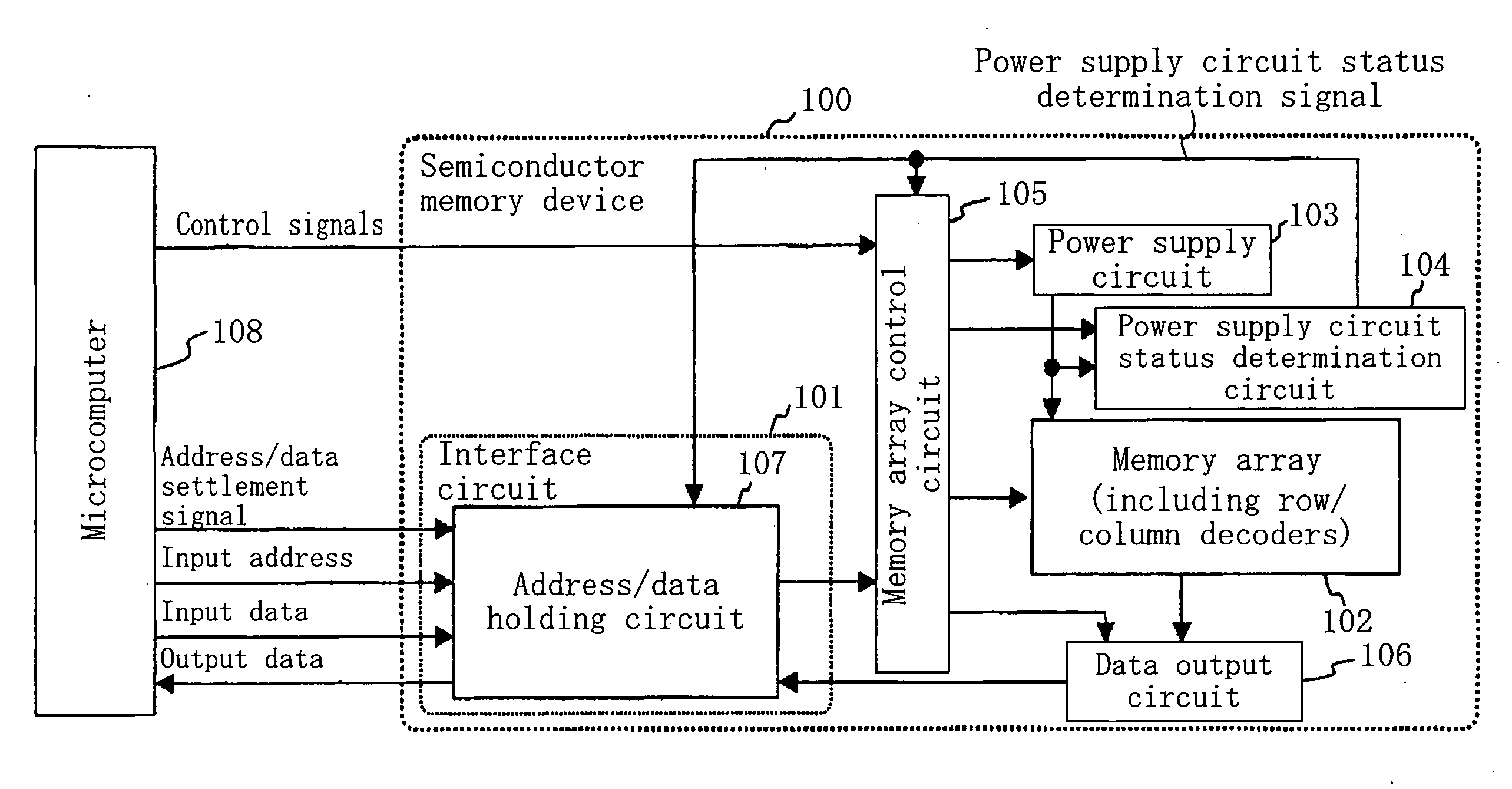
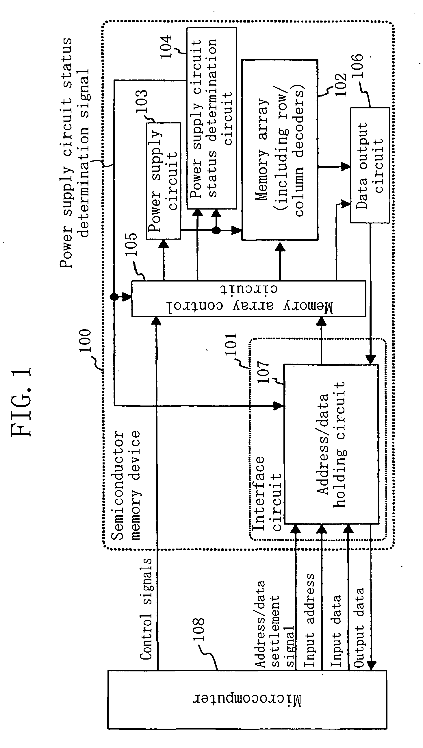
[0033]Referring to FIG. 1, the semiconductor memory device 100 includes an interface circuit 101, a memory array 102, a power supply circuit 103 having a voltage boosting function, a power supply circuit status determination circuit 104, a memory array control circuit 105, and a data output circuit 106.

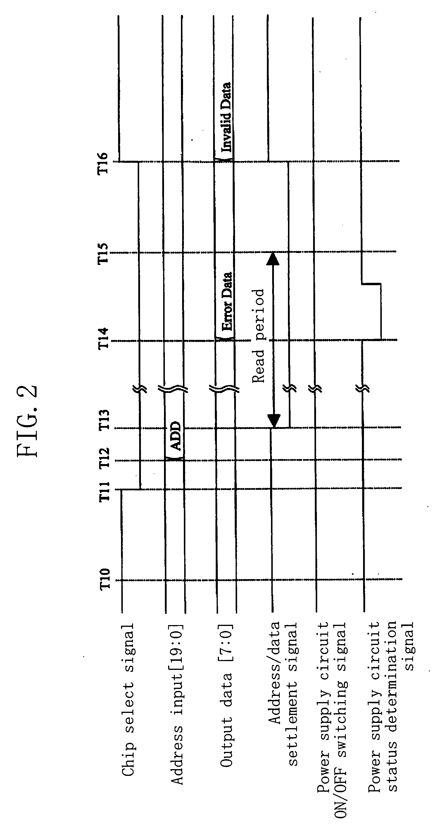
[0034]The semiconductor memory device 100 receives, from a microcomputer 108, a plurality of control signals for controlling the semiconductor memory device 100, an address / data settlement signal, an input address, and input data. The plurality of control signals include a chip select signal, and a power supply circuit ON / OFF switching signal. The semiconductor memory device 100 outputs output data to the microcomputer 108. These signals are exchanged between the semiconductor memory device 100 and the microcomputer 108 in parallel transmission as shown in FIG. 1.

[0035]The chip select signal is a signal for controlling the validity of a read operation, a write operation, or the like o...

embodiment 2

[0050]Referring to FIG. 3, a semiconductor memory device 200 of Embodiment 2 includes an interface circuit 201, a command interpretation circuit 202, the memory array 102, the power supply circuit 103 having a voltage boosting function, the power supply circuit status determination circuit 104, a memory array control circuit 205, and the data output circuit 106. The interface circuit 201 includes a clock counter circuit 203 and an address / data holding circuit 207.

[0051]The semiconductor memory device 200 receives, from a microcomputer 208, a plurality of control signals for controlling the semiconductor memory device 200, a clock signal, an input address, and input data. The plurality of control signals include a chip select signal. The semiconductor memory device 200 outputs output data to the microcomputer 208. In the present embodiment, the input address, the input data and the output data are exchanged between the semiconductor memory device 200 and the microcomputer 208 in seri...

embodiment 3

[0067]Referring to FIG. 5, a semiconductor memory device 300 of Embodiment 3 includes an interface circuit 301, the memory array 102, the power supply circuit 103 having a voltage boosting function, the power supply circuit status determination circuit 104, a memory array control circuit 305, and the data output circuit 106. The interface circuit 301 includes an address / data control circuit 302 and an address / data holding circuit 307.

[0068]The semiconductor memory device 300 receives, from a microcomputer 108, a plurality of control signals for controlling the semiconductor memory device 300, an address / data settlement signal, an input address, and input data. The plurality of control signals include a chip select signal, and a power supply circuit ON / OFF switching signal. The semiconductor memory device 300 outputs output data to the microcomputer 108. These signals are exchanged between the semiconductor memory device 300 and the microcomputer 108 in parallel transmission as shown...


PUM


Abstract

A semiconductor memory device includes: a power supply circuit for outputting a power supply voltage used for reading out data; and a power supply circuit status determination circuit for determining whether an operation status of the power supply circuit is such that data can be read out normally. The output of readout data is suppressed while it is determined by the power supply circuit status determination circuit that the operation status is such that data cannot be read out normally.

Description

CROSS REFERENCE TO RELATED APPLICATION[0001]This application claims priority under 35 U.S.C. § 119 on Patent Application No. 2006-094029 filed in Japan on Mar. 30, 2006, the entire contents of which are hereby incorporated by reference.BACKGROUND OF THE INVENTION[0002]1. Field of the Invention[0003]The present invention relates to a semiconductor memory device and, more particularly, to a semiconductor memory device in which a voltage output by a power supply circuit having a voltage booster circuit is used for reading out stored data.[0004]2. Description of the Background Art[0005]A conventional non-volatile semiconductor memory as shown in FIG. 3 of Japanese Laid-Open Patent Publication No. 2003-132691 is known in the art. The non-volatile semiconductor memory outputs a ready_to_read signal, which is a logical product of two signals, one indicating that a read charge pump has been charged up after the rising of the power supply voltage, and another indicating that a predetermined ...

Claims


Application Information

Patent Timeline
Patent Type & Authority Applications(United States)
IPC IPC(8): G11C5/14
CPCG11C5/143G11C16/34G11C5/14G11C7/10
Inventor NITTA, TADASHINISHIKAWA, KAZUYOUEMINAMI, MASAHIRO
Owner CETUS TECH INC
Why Eureka
Try Eureka