Manufacturing method of a semiconductor device

a manufacturing method and technology of a semiconductor device, applied in the direction of semiconductor/solid-state device manufacturing, basic electric elements, electric devices, etc., can solve the problems of wafer to divide into chips, and large stress applied to the wafer, so as to achieve the improvement of the reliability of the semiconductor device, the effect of preventing the shift and movement of the semiconductor chip and preventing the generation of chipping

Inactive Publication Date: 2007-11-29
RENESAS ELECTRONICS CORP
View PDF8 Cites 24 Cited by
  • Summary
  • Abstract
  • Description
  • Claims
  • Application Information

AI Technical Summary

Benefits of technology

[0019]Since the adhesive layer (paste) of the dicing tape is hardened and subsequently the semiconductor wafer is bent, shifting and movement of the semiconductor chip can be prevented because the paste has hardened at the time of the bending. As a result, generation of chipping can also be inhibited and improvement in the reliability of a semiconductor device can be attained.
[0020]...

Problems solved by technology

The reason to do so is not to allow the chips being prepared as individual chips by dicing to disperse away from the dicing tape due to vibration of the dicing blade.
However, in the blade dicing method, a stress applied to the wafer is large as compared to the laser dicing method.
Therefore, as a semiconductor wa...

Method used


Image

  • Manufacturing method of a semiconductor device
  • Manufacturing method of a semiconductor device
  • Manufacturing method of a semiconductor device

Examples


first embodiment

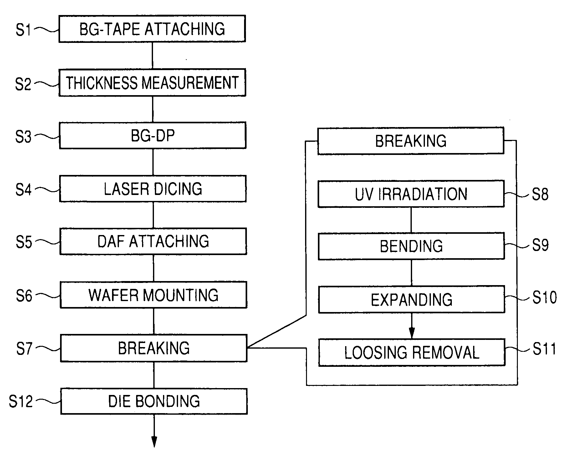
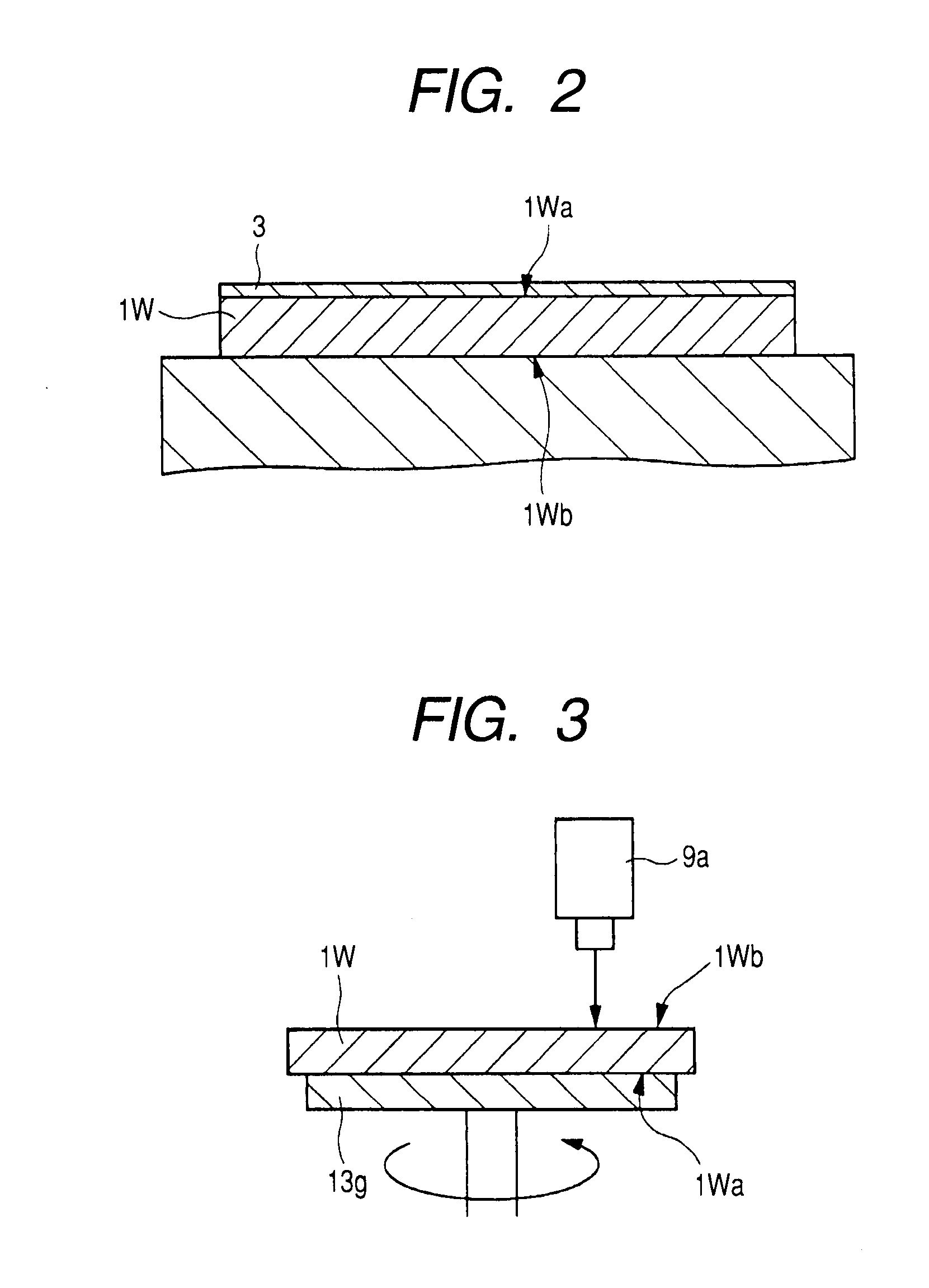
[0050]FIG. 1 is a flow diagram showing one example of a manufacturing method of a semiconductor device of a first embodiment of this invention; FIG. 2 is a sectional view showing one example of a BG-tape attached state in the flow shown in FIG. 1; FIG. 3 is a conceptual diagram showing one example of a state of thickness measurement of the wafer in the flow shown in FIG. 1; FIG. 4 is a conceptual diagram showing one example of a wafer thickness measuring instrument in the flow shown in FIG. 1; and FIG. 5 is a conceptual diagram showing one example of an output waveform of the thickness measuring instrument shown in FIG. 4. Moreover, FIG. 6 is a plan view showing one example of a construction of backside BG equipment in the flow shown in FIG. 1; FIG. 7 is a conceptual diagram showing one example of a backside grinding state in the flow shown in FIG. 1; FIG. 8 is a conceptual diagram showing one example of a laser dicing state in the flow shown in FIG. 1; FIG. 9 is a sectional diagram...

second embodiment

[0091]FIG. 20 is a flow diagram showing one example of a manufacturing method of a semiconductor device of a second embodiment of this invention. FIG. 21 is a sectional view showing one example of a wafer mount state in the flow shown in FIG. 20. FIG. 22 is a sectional view showing one example of a UV irradiation state in the flow shown in FIG. 20; FIG. 23 is a sectional view showing one example of an expanding state in the flow shown in FIG. 20, and FIG. 24 is a sectional view showing one example of a picking-up state in the manufacturing method of a semiconductor device of the second embodiment of this invention.

[0092]The manufacturing method of a semiconductor device of this second embodiment, like the first embodiment, relates to assembly of a semiconductor device with a mounted thin semiconductor chip of a chip thickness of 50 μm or less. A point different from the first embodiment is that, in mounting the wafer on the dicing tape 5, the semiconductor wafer 1W is directly mount...


PUM


Abstract

This invention aims at improvement in reliability of a semiconductor device. In this invention, a semiconductor wafer is irradiated with laser light so as to have a fractured layer formed in the interior of the semiconductor wafer, the semiconductor wafer is mounted on a dicing tape via paste (adhesive layer), then the paste of the dicing tape is hardened by UV irradiation or cooling, and subsequently the semiconductor wafer is bent (breaking). By this process, shifting and movement of semiconductor chips can be prevented because the paste has been hardened at the time of the bending. As a result, the semiconductor chip can be prevented from interfering with adjacent chips and can also be inhibited from generating chipping; therefore, the reliability of a semiconductor device can be improved.

Description

CROSS-REFERENCE TO RELATED APPLICATION[0001]The present application claims priority from Japanese patent application No. 2006-93300 filed on Mar. 30, 2006, the content of which is hereby incorporated by reference into this application.BACKGROUND OF THE INVENTION[0002]The present invention relates to a manufacturing technology of a semiconductor device and, more particularly, to a manufacturing method of a semiconductor device that uses a dicing tape.[0003]There exists a technology that is specified to have a process of mounting a wafer with a protection sheet attached thereon and with a backside being ground to a very thin thickness on a first ring frame via a first adhesive sheet with its backside facing the outside and dicing the wafer in this state from the backside, and a process of turning the diced wafer upside down and attaching it again to a second ring frame via a second adhesive sheet (for example, see Japanese Unexamined Patent Publication No. 2005-228794 (FIG. 1)).SUMMAR...

Claims


Application Information

Patent Timeline
IPC IPC(8): H01L21/78
CPCH01L21/78H01L21/30
Inventor ABE, YOSHIYUKIMUTO, HIDEO
Owner RENESAS ELECTRONICS CORP
Why Eureka
Try Eureka