Method of manufacturing flash memory device

a flash memory and manufacturing method technology, applied in the direction of semiconductor devices, basic electric elements, electrical appliances, etc., can solve the problems of reduced contact hole size, high yield loss, and difficulty in securing the bridge margin between the contacts, so as to improve the bridge

Inactive Publication Date: 2007-11-29
SK HYNIX INC
View PDF9 Cites 0 Cited by
  • Summary
  • Abstract
  • Description
  • Claims
  • Application Information

AI Technical Summary

Benefits of technology

[0008]Accordingly, the invention addresses the above problems, and provides a method of manufacturing a flash memory device, in which a contact hole of a square form is formed through a dual mask process of a line fashion employing a hard mask layer, improving the bridge occurring between the contacts.

Problems solved by technology

It reduces the size of the contact hole and thus makes it difficult to secure the bridge margin between the contacts.
Accordingly, the loss of the yield, which is incurred by one drain contact bridge, is very high.

Method used


Image

  • Method of manufacturing flash memory device
  • Method of manufacturing flash memory device
  • Method of manufacturing flash memory device

Examples


Embodiment Construction

[0013]Specific embodiments according to the invention will be described with reference to the accompanying drawings.

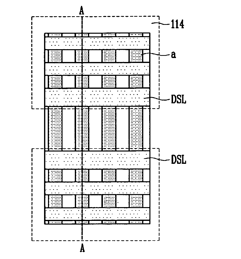
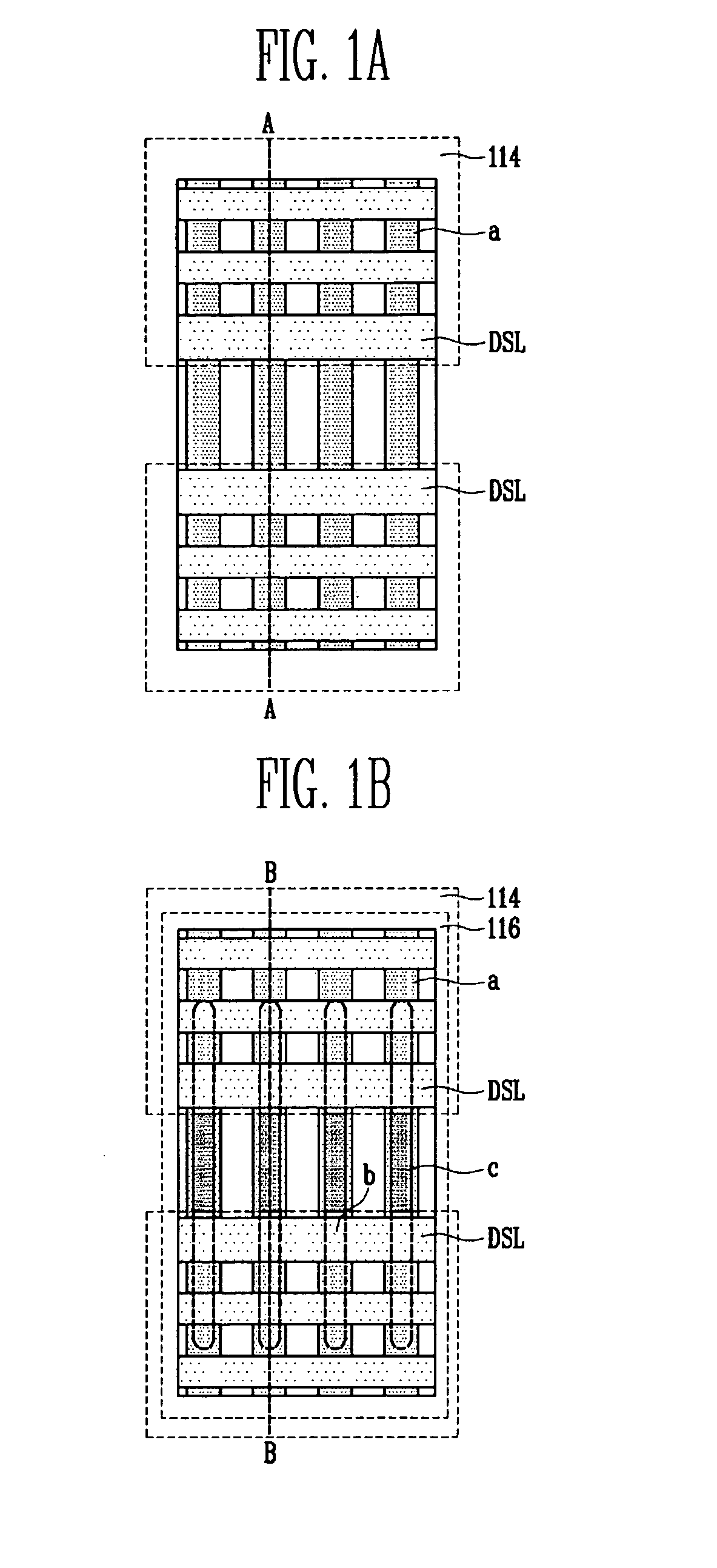
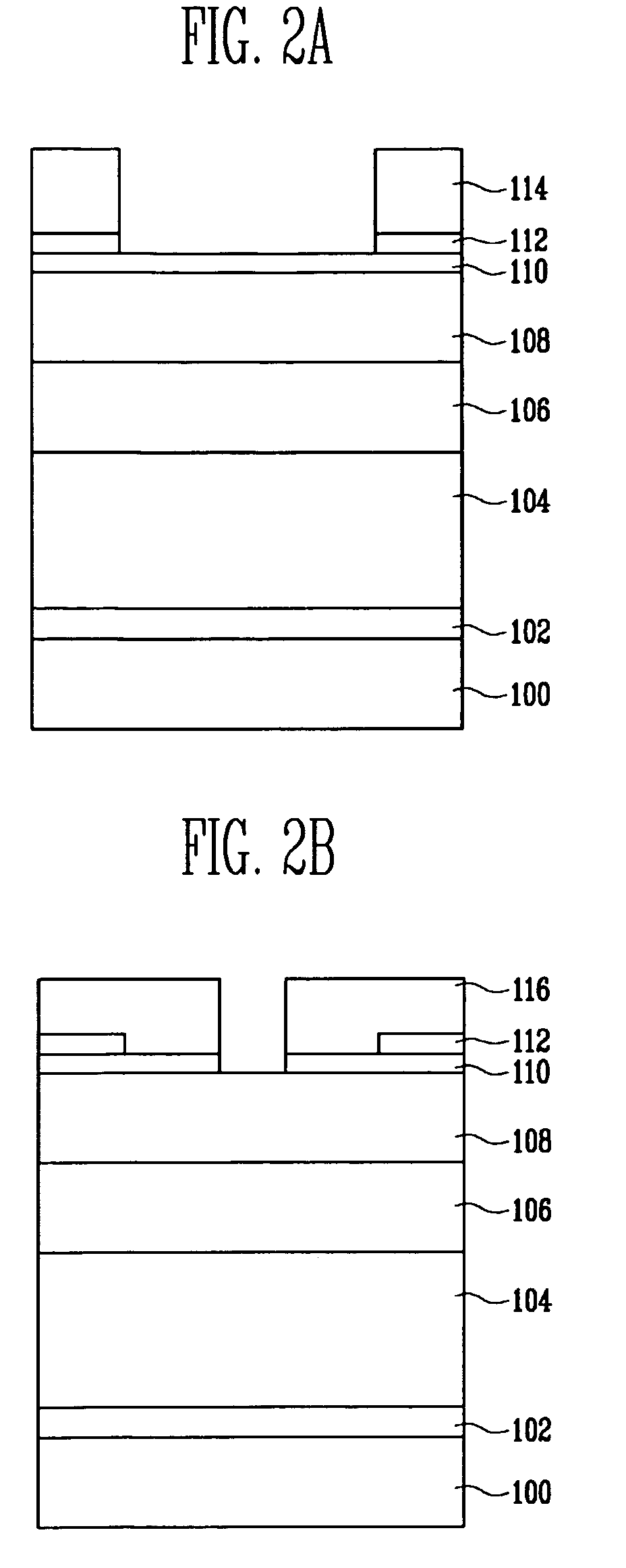
[0014]Referring to FIGS. 1A and 2A, an etch-prevention layer 102 and a first interlayer insulating layer 104 are sequentially formed on a semiconductor substrate 100 in which predetermined structures such as an isolation layer, agate, a spacer, a self-aligned contact (SAC) nitride layer, etc. are formed. Chemical mechanical polishing (CMP) is then performed. The etch-prevention layer 102 may be formed using a nitride layer, and the first interlayer insulating layer 104 may be formed using a high-density plasma (HDP) oxide layer. The first interlayer insulating layer 104 and the etch-prevention layer 102 are etched by photo and etch processes, forming a source contact hole (not shown).

[0015]A first polysilicon layer is deposited on the entire surface so that the source contact hole is gap filled. The first polysilicon layer is polished so that the first interlayer insul...


PUM


Abstract

A method of manufacturing a flash memory device which an etch-prevention layer, first and second interlayer insulating layers, and first, second and third hard mask layers are sequentially formed on a semiconductor substrate. The third hard mask layer is etched to expose a portion of a region on the second hard mask layer. A photoresist pattern of a line shape is formed on the entire surface such that the photoresist pattern is exposed to be narrower than the region through which the second hard mask layer is exposed. The second hard mask layer is etched using the photoresist pattern as a mask. The first hard mask layer is etched using the photoresist pattern as a mask, and the second and first interlayer insulating layers are then etched using the remaining third and second hard mask layers as masks, thus forming a drain contact hole having a square shape. The etch-prevention layer is etched using the remaining second and first hard mask layers as masks, thereby exposing a predetermined region of the semiconductor substrate and opening the drain contact hole. It is thus possible to improve a bridge occurring between the contacts.

Description

BACKGROUND[0001]1. Field of the Invention[0002]The invention relates, in general, to flash memory devices and, more particularly, to a method of manufacturing a flash memory device, in which a contact hole of a square shape is formed through a dual mask process of a line fashion employing a hard mask layer, thus improving a bridge occurring between contacts.[0003]2. Discussion of Related Art[0004]In the formation method of the drain contact hole of a flash memory device, if an exposure process using ArF having a low wavelength as a light source in order to form micro patterns of 70 nm or less is performed using a photoresist (PR), Contact Edge Roughness (CER) of the patterns is degraded. Accordingly, spacer margin between patterns is reduced when the micro patterns are formed, causing a bridge between the patterns.[0005]More particularly, since the space width between the contact holes on the layout is small, the etch selectivity is lowered when the drain contact hole is formed. Are...

Claims


Application Information

Patent Timeline
Patent Type & Authority Applications(United States)
IPC IPC(8): H01L21/302
CPCH01L27/115H01L27/11565H01L27/11519H01L27/11517H10B41/10H10B41/00H10B43/10H10B69/00H01L29/40114H01L29/40117
Inventor LEE, SUNG HOON
Owner SK HYNIX INC
Why Eureka
Try Eureka