Built-in system and method for testing integrated circuit timing parameters

a timing parameter and integrated circuit technology, applied in the field of integrated circuit devices, can solve the problems of difficult to test the timing characteristics of the integrated circuit, the testing environment is not without limitations and disadvantages, and the memory device is more difficult to position the transition of the dqs

Active Publication Date: 2007-12-06
MICRON TECH INC
View PDF1 Cites 22 Cited by
  • Summary
  • Abstract
  • Description
  • Claims
  • Application Information

AI Technical Summary

Problems solved by technology

As the length of the data hold period gets smaller, it becomes more difficult for the memory device to position transitions of the DQS signal at the start of the data valid period.
However, the testing environment is not without its limitations and disadvantages.
For example, it is very difficult to test various timing characteristics of the integrated circuits, particularly at the high operating speeds for which such integrated circuits are designed.
This difficulty in testing timing characteristics results primarily from the propagation delays in the cable coupling the tester to the test head.
The cables that are typically used in such testing environments are often fairly long, thus making the delays of signals coupled to and from the integrated circuits correspondingly long and often difficult to predict.
Another problem with the above-described testing environment is that it may not accurately simulate the conditions in which the integrated circuits will actually be used.
In particular, the integrated circuits, and particularly the timing parameters of integrated circuits, are not generally tested during use in an actual operating environment and after a substantial period has lapsed.
Therefore, even if the timing parameters of the integrated circuit were within specification when the integrated circuit was shipped from a fabrication facility, there can be no assurance that the timing parameters are within a specified range during use, particularly after a substantial period of time.
Also, it is difficult to measure a skew between two output ports as opposed to measuring a skew between an input port and an output port.

Method used


Image

  • Built-in system and method for testing integrated circuit timing parameters
  • Built-in system and method for testing integrated circuit timing parameters
  • Built-in system and method for testing integrated circuit timing parameters

Examples


Embodiment Construction

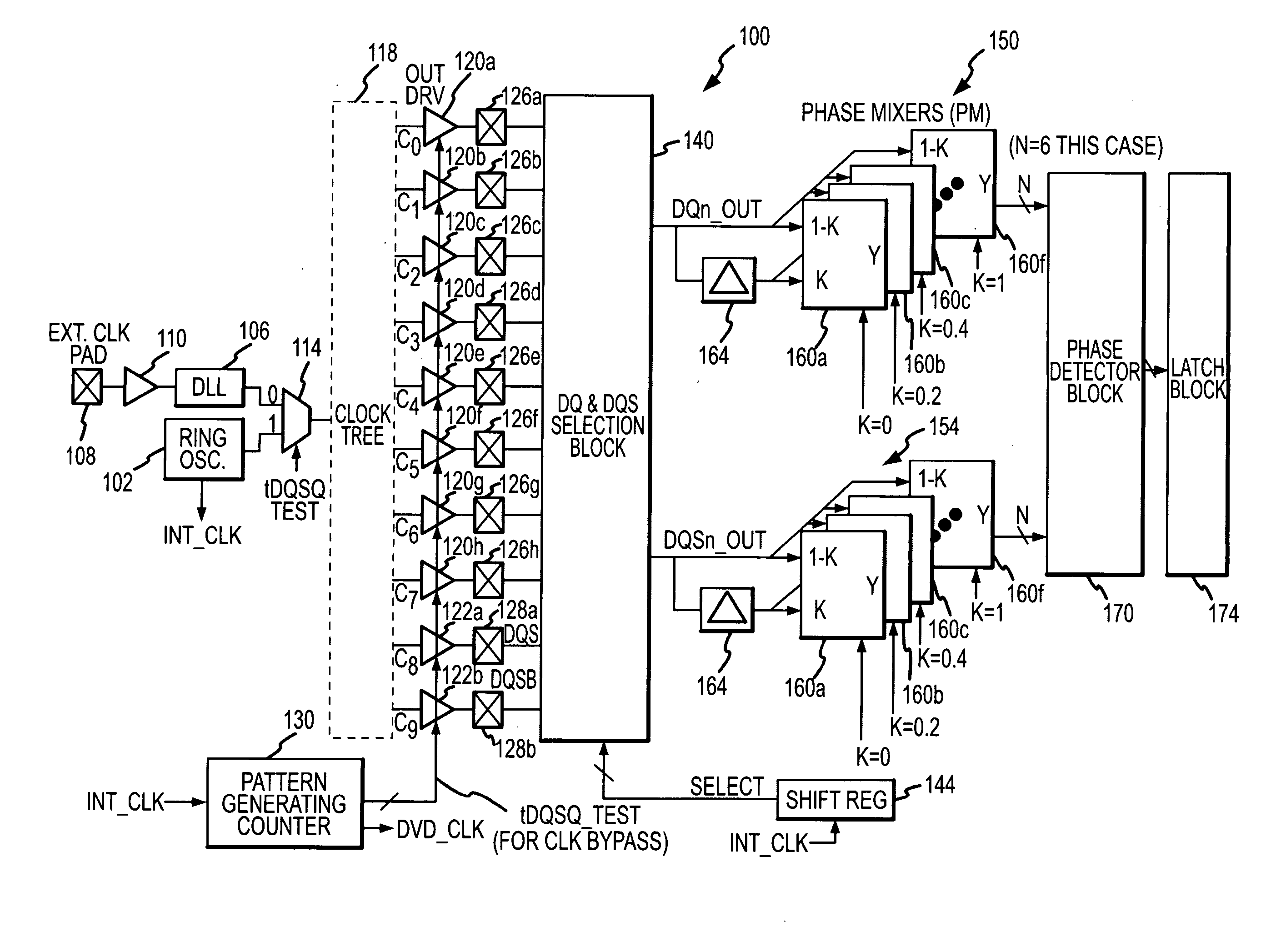
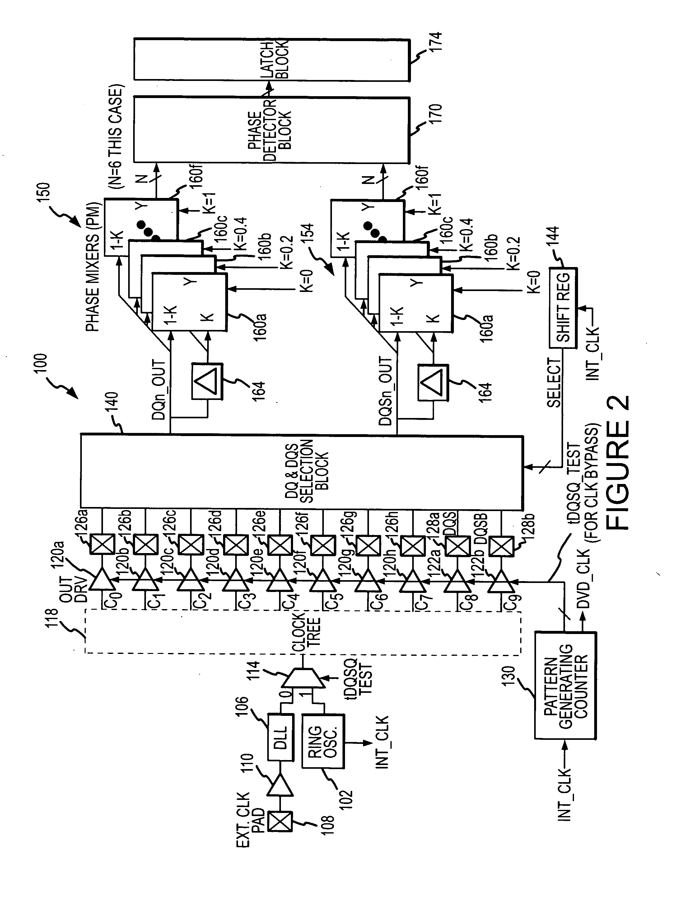
[0014] A built-in self-test system 100 according to one example of the invention is shown in FIG. 2. The self-test system 100 is preferably fabricated on the same substrate as a memory device (not shown) being tested, although other configurations may also be used. The system 100 includes a ring oscillator 102 that generates a periodic clock signal that is used during testing. During normal operation, a clock signal is generated by a delay-lock loop 106 responsive to an external clock signal applied to an external terminal pad 108 and coupled through a driver 110. The advantage of using an internal oscillator is that it may be possible to make the frequency of the clock signal higher than the frequency of an externally applied clock signal. A multiplexer 114 responds to a tDQSQ test signal to select as an output clock signal the output of the delay-lock loop 106 during normal operation and the output of the ring oscillator 102 during memory device testing. The ring oscillator 102 al...


PUM


Abstract

A built-in self-test system for a dynamic random access memory device using a data output register of the memory device to apply test signals to data bus terminals and a data strobe terminal of the memory device responsive to respective clock signals. The clock signal are generated by a test system oscillator and coupled through a clock tree of the memory device. The test system further includes a selector that sequentially selects each of the test signals applied to the data bus terminals and applies the selected test signal to a multi-phase generator. The multi-phase generator delays the selected signal by different time to generate a set of delayed signals. The phases of the delayed signals are compared to the test signal applied to the data strobe terminal to determine the delay of the compared signals relative to each other, thereby determining the timing parameter.

Description

TECHNICAL FIELD [0001] This invention relates to integrated circuit devices such as memory devices, and, more particularly, to a method and system included in an integrated circuit for testing timing parameters in the integrated circuit device. BACKGROUND OF THE INVENTION [0002] During the fabrication of integrated circuits such as memory devices, it is conventional to test such integrated circuits at several stages during the fabrication process. For example, the integrated circuits are normally connected to a tester with a probe card when the integrated circuits are still in wafer form. In a final test occurring after the integrated circuits have been diced from the wafer and packaged, the integrated circuits are placed into sockets on a load board. The load board is then placed on a test head, typically by a robotic handler. The test head makes electrical contact with conductors on the load board that are connected to the integrated circuits. The test head is connected through a ...

Claims


Application Information

Patent Timeline
Patent Type & Authority Applications(United States)
IPC IPC(8): G11C29/00H03L7/00G01R23/175G11C7/00G11C8/00
CPCG01R31/3016G01R31/31727G11C7/22G11C7/222G11C29/50012G11C11/401G11C29/12015G11C29/50G11C8/10
Inventor KWAK, JONGTAE
Owner MICRON TECH INC
Why Eureka
Try Eureka