N-channel mosfets comprising dual stressors, and methods for forming the same

a technology of metaloxidesemiconductor and stressor, which is applied in the field of nchannel metaloxidesemiconductor field effect transistors (nmosfets) having dual stressors, to achieve the effect of improving the stress profil

Active Publication Date: 2007-12-06
AURIGA INNOVATIONS INC
View PDF17 Cites 25 Cited by
  • Summary
  • Abstract
  • Description
  • Claims
  • Application Information

AI Technical Summary

Benefits of technology

[0007] The present invention provides an n-channel field effect transistor (n-FET) comprising dual stressors for applying desired tensile stress to the channel region of the n-FET. The dual stressors in the n-FET of the present invention provide an improved stress profile in the channel region of the n-FET, without otherwise compromising the device performance of the n-FET.

Problems solved by technology

The use of such a strain-inducing SiGe layer has several inherent disadvantages: (1) formation of relaxed SiGe buffer layer relies on defect formation, and consequentially, the SiGe material has a high defect density, which propagates into the silicon channel layer thereabove and poses significant challenges for device applications, such as control of leakage current and device yield, and (2) the presence of the SiGe layer directly underneath the channel region creates processing issues, such as deleterious diffusion of germanium into the strained silicon channel, high resistance silicide formation and altered dopant diffusion.

Method used


Image

  • N-channel mosfets comprising dual stressors, and methods for forming the same
  • N-channel mosfets comprising dual stressors, and methods for forming the same
  • N-channel mosfets comprising dual stressors, and methods for forming the same

Examples


Embodiment Construction

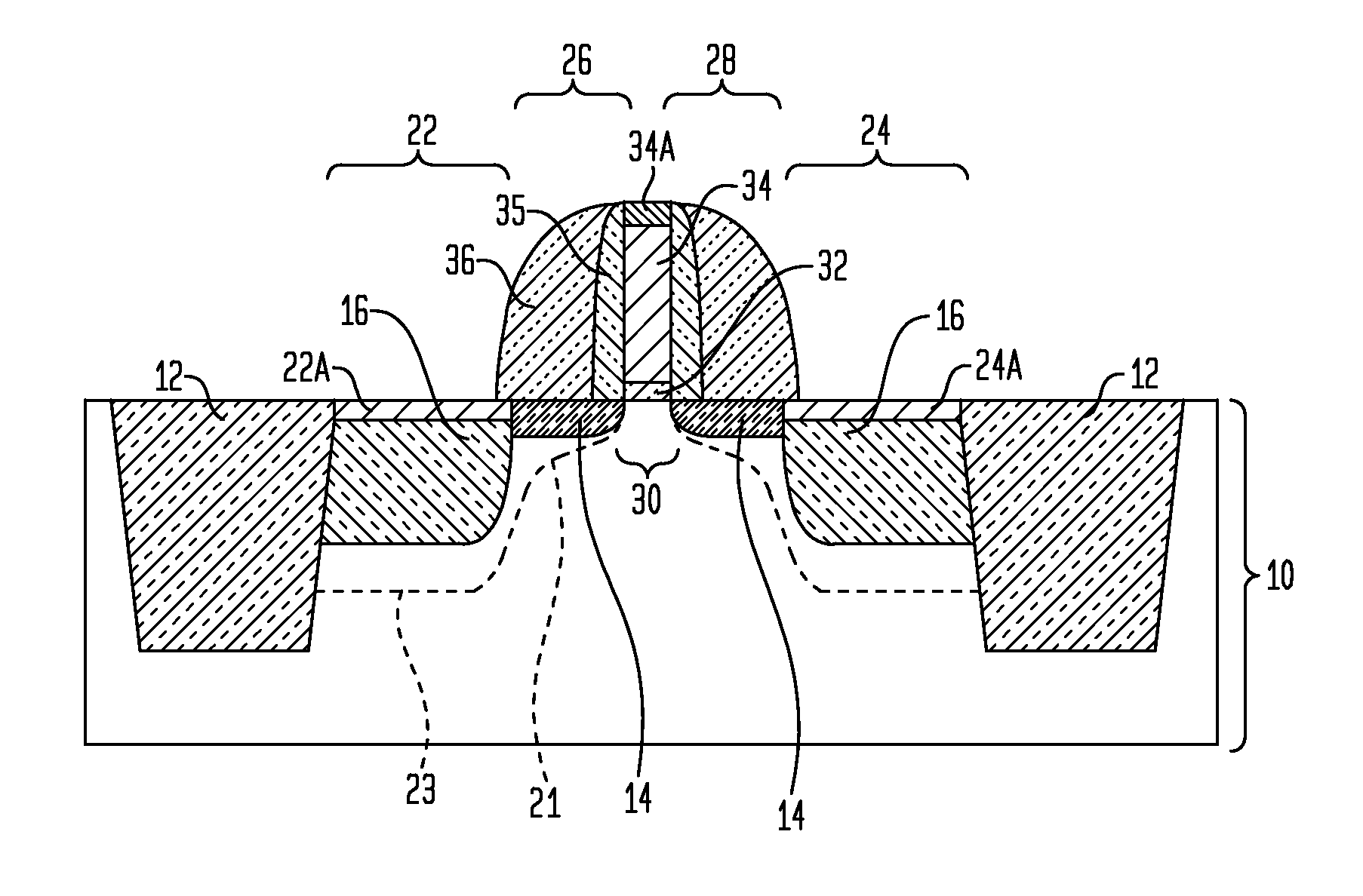
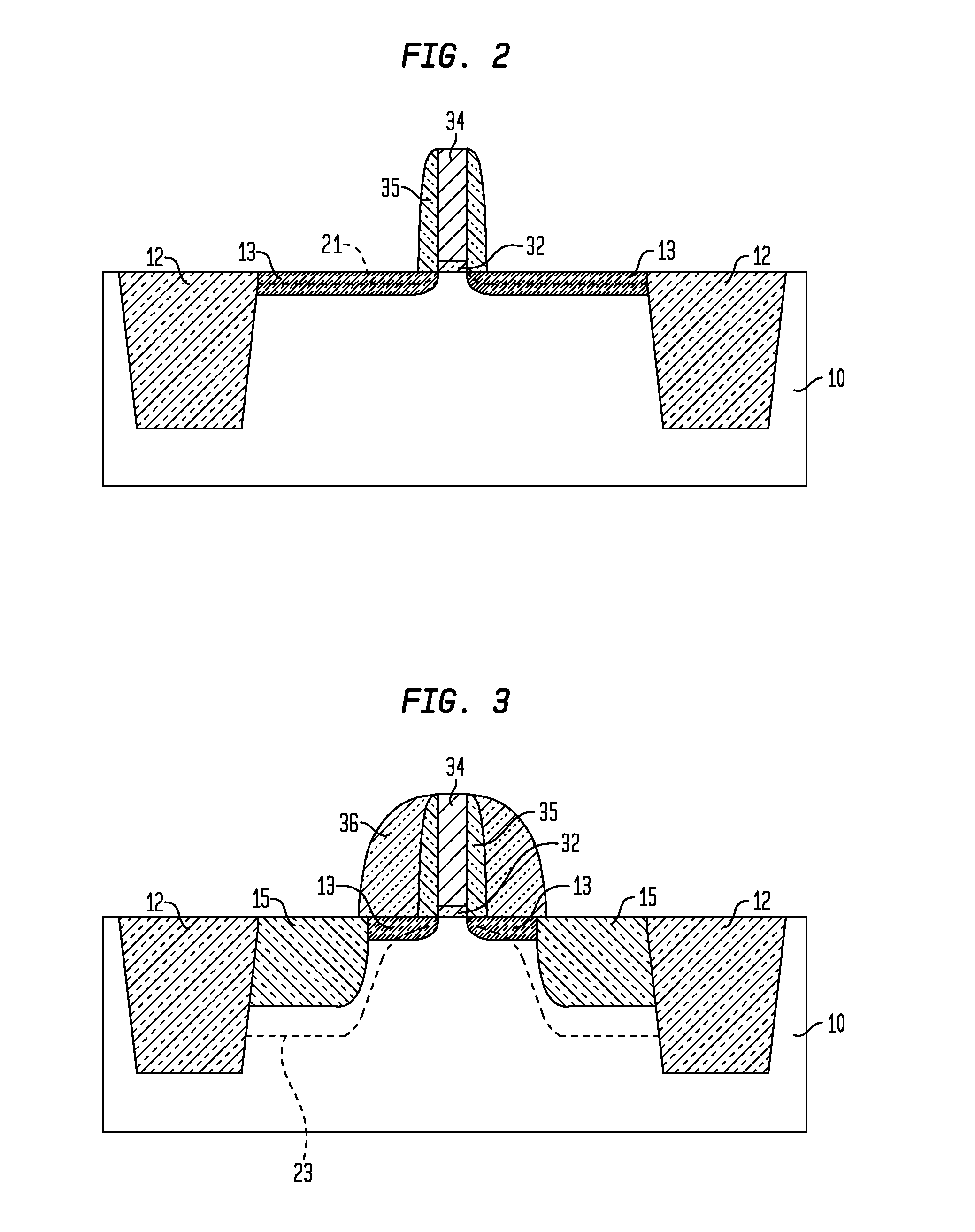
[0025] In the following description, numerous specific details are set forth, such as particular structures, components, materials, dimensions, processing steps and techniques, in order to provide a thorough understanding of the present invention. However, it will be appreciated by one of ordinary skill in the art that the invention may be practiced without these specific details. In other instances, well-known structures or processing steps have not been described in detail in order to avoid obscuring the invention.

[0026] It will be understood that when an element as a layer, region or substrate is referred to as being “on” another element, it can be directly on the other element or intervening elements may also be present. In contrast, when an element is referred to as being “directly on” another element, there are no intervening elements present. It will also be understood that when an element is referred to as being “connected” or “coupled” to another element, it can be directl...


PUM

PropertyMeasurementUnit
depthaaaaaaaaaa
depthaaaaaaaaaa
depthaaaaaaaaaa

Abstract

The present invention relates to a semiconductor device comprising at least one n-channel field effect transistor (n-FET). Specifically, the n-FET comprises first and second patterned stressor layers that both contain a carbon-substituted and tensilely stressed single crystal semiconductor. The first patterned stressor layer has a first carbon concentration and is located in source and drain (S / D) extension regions of the n-FET at a first depth. The second patterned stressor layer has a second, higher carbon concentration and is located in S / D regions of the n-FET at a second, deeper depth. Such an n-FET with the first and second patterned stressor layers of different carbon concentration and different depths provide improved stress profile for enhancing electron mobility in the channel region of the n-FET.

Description

RELATED APPLICATIONS [0001] This application is a divisional application of U.S. Ser. No. 11 / 420,047 filed May 24, 2006.FIELD OF THE INVENTION [0002] The present invention relates to complementary metal-oxide-semiconductor (CMOS) devices with enhanced carrier mobility. More specifically, the present invention relates to n-channel metal-oxide-semiconductor field effect transistors (n-MOSFETs) having dual stressors for enhancing electronic mobility in channel regions of such n-MOSFETs. BACKGROUND OF THE INVENTION [0003] Mechanical stresses within a semiconductor device substrate can be used to modulate device performance. For example, in silicon, hole mobility is enhanced when the silicon film is under compressive stress, while the electron mobility is enhanced when the silicon film is under appropriate tensile stress. Therefore, compressive or tensile stress can be advantageously created in the channel region of a p-MOSFET or an n-MOSFET in order to enhance the performance of such a ...

Claims


Application Information

Patent Timeline
Patent Type & Authority Applications(United States)
IPC IPC(8): H01L21/8238
CPCH01L21/26506H01L21/324H01L21/823807H01L21/823814H01L29/665Y10S257/90H01L29/6659H01L29/66636H01L29/7833H01L29/7848H01L29/6656
Inventor LI, JINGHONG H.LIU, YAOCHENGLUO, ZHIJIONGMADAN, ANITAROVEDO, NIVO
Owner AURIGA INNOVATIONS INC
Why Eureka
Try Eureka