Mitigation of edge degradation in ferroelectric memory devices through plasma etch clean

a technology of ferroelectric memory and edge degradation, which is applied in the field of integrated circuit processing, can solve the problems of personal devices requiring more computational power and on-chip memory read operation is destructive, etc., and achieves the effects of reducing polarization, facilitating ferroelectric memory device operation and fabrication, and reducing edge defects and performance degradation of fabricated ferroelectric memory cells

Active Publication Date: 2007-12-06
TEXAS INSTR INC
View PDF8 Cites 10 Cited by
  • Summary
  • Abstract
  • Description
  • Claims
  • Application Information

AI Technical Summary

Benefits of technology

[0012]Aspects of the present invention facilitate ferroelectric memory device operation and fabrication by mitigating edge degradation of ferroelectric memory cells, which can result in signal degradation, reduced polarization, and / or failure. Aspects of the present invention employ a plasma based dry clean during and / or after ferroelectric stack etching, which can mitigate edge defects and performance degradation of fabricated ferroelectric memory cells.
[0013]In accordance with an aspect of the invention, a method of forming a ferroelectric memory device is disclosed. A bottom electrode diffusion barrier layer is formed over one or more semiconductor layers, such as an interlevel dielectric layer. A bottom electrode layer is then formed over the bottom electrode diffusion barrier layer. A ferroelectric layer is formed over the bottom electrode. A top electrode is formed over the ferroelectric layer. The top electrode, the ferroelectric layer, and the bottom electrode are patterned or etched. A dry clean is performed that mitigates edge degradation. The dry clean can remove debris and form residual compounds for later removal. A wet etch / clean is then performed that can remove the residual compounds.

Problems solved by technology

In addition to being smaller and more portable, personal devices are requiring more computational power and on-chip memory.
A characteristic of the shown ferroelectric memory cell is that a read operation is destructive.
If the polarization of the ferroelectric is switched, the read operation is destructive and the sense amplifier must rewrite (onto that cell) the correct polarization value as the bit just read from the cell.
One problem encountered by ferroelectric memory is signal degradation during read and write operations.
The signal degradation can result in sense amplifiers being unable to determine storage states for affected ferroelectric memory cells.
As a result, such ferroelectric memory cells can become unusable.

Method used


Image

  • Mitigation of edge degradation in ferroelectric memory devices through plasma etch clean
  • Mitigation of edge degradation in ferroelectric memory devices through plasma etch clean
  • Mitigation of edge degradation in ferroelectric memory devices through plasma etch clean

Examples


Embodiment Construction

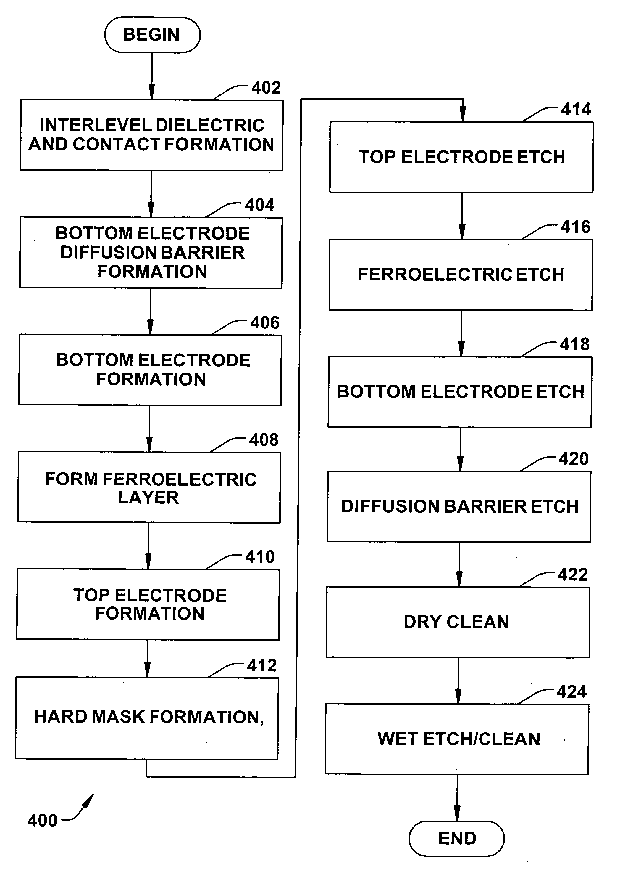
[0026]The present invention will now be described with respect to the accompanying drawings in which like numbered elements represent like parts. The figures provided herewith and the accompanying description of the figures are merely provided for illustrative purposes. One of ordinary skill in the art should realize, based on the instant description, other implementations and methods for fabricating the devices and structures illustrated in the figures and in the following description.

[0027]Aspects of the present invention facilitate ferroelectric memory device operation and fabrication by mitigating edge degradation of ferroelectric memory cells, which can result in signal degradation, reduced polarization, and / or failure. Aspects of the present invention employ a plasma based dry clean during and / or after ferroelectric stack etching, which can mitigate edge defects and performance degradation of fabricated ferroelectric memory cells.

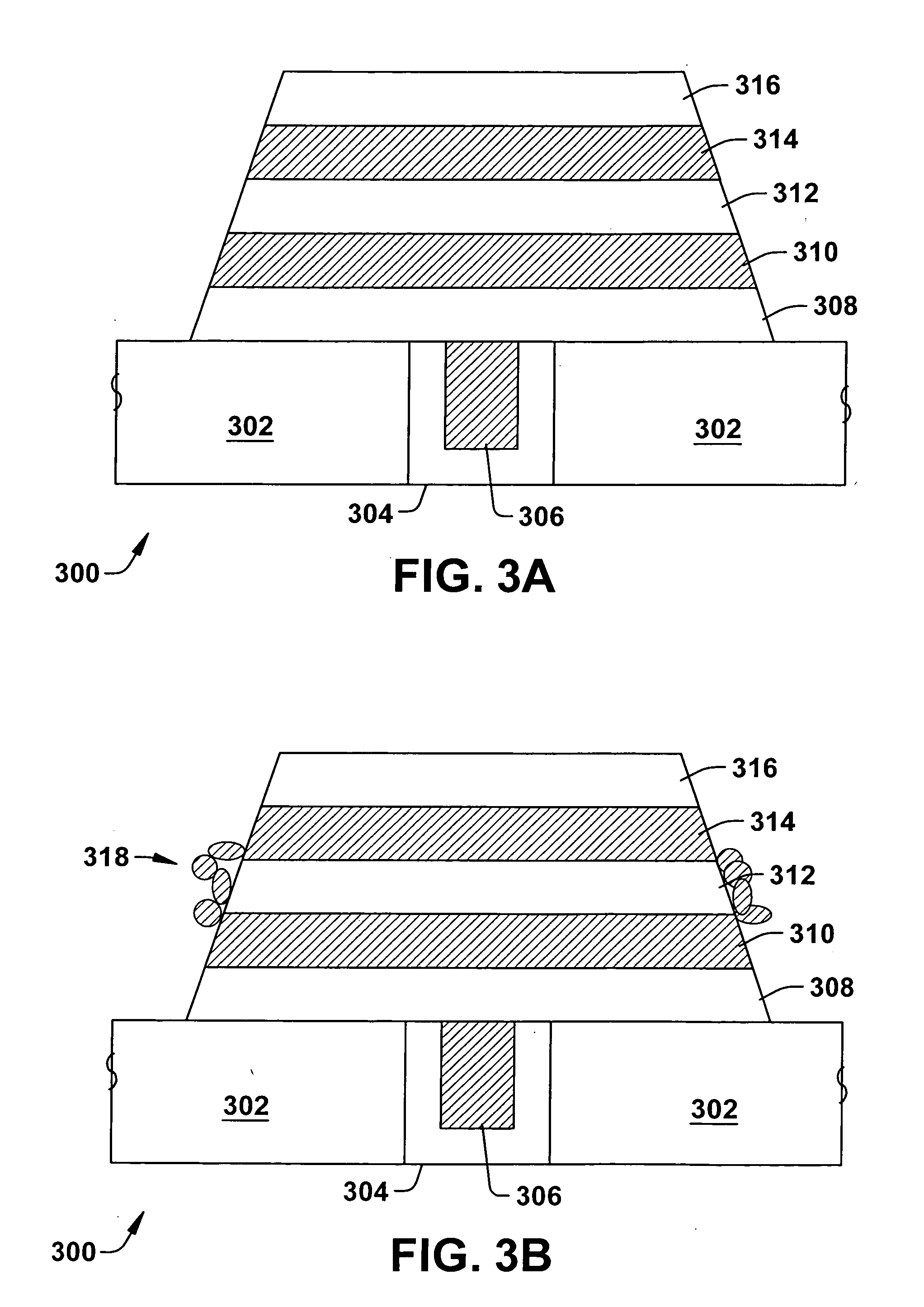
[0028]FIG. 3A is a cross sectional view of a fe...


PUM


Abstract

A ferroelectric memory device is fabricated while mitigating edge degradation. A bottom electrode is formed over one or more semiconductor layers. A ferroelectric layer is formed over the bottom electrode. A top electrode is formed over the ferroelectric layer. The top electrode, the ferroelectric layer, and the bottom electrode are patterned or etched. A dry clean is performed that mitigates edge degradation. A wet etch/clean is then performed.

Description

FIELD OF THE INVENTION[0001]The present invention relates generally to the field of integrated circuit processing, and more particularly, to fabrication of ferroelectric memory devices employing a dry clean to mitigate edge degradation.BACKGROUND OF THE INVENTION[0002]Several trends exist, today, in the semiconductor device fabrication industry and the electronics industry. Devices are continuously getting smaller and smaller and requiring less and less power. A reason for this is that more personal devices are being fabricated which are very small and portable, thereby relying on a small battery as its supply source. For example, cellular phones, personal computing devices, and personal sound systems are devices which are in great demand in the consumer market. In addition to being smaller and more portable, personal devices are requiring more computational power and on-chip memory. In light of all these trends, there is a need in the industry to provide a computational device whic...

Claims


Application Information

Patent Timeline
Patent Type & Authority Applications(United States)
IPC IPC(8): H01L21/336
CPCH01L21/0206H01L21/02071H01L21/31122H01L28/65H01L27/11502H01L28/55H01L21/32136H10B53/00
Inventor UDAYAKUMAR, KEZHAKKEDATH R.HALL, LINDSEY H.CELII, FRANCIS G.SUMMERFELT, SCOTT R.
Owner TEXAS INSTR INC
Why Eureka
Try Eureka