Semiconductor device and method for fabricating the same

a technology of semiconductor devices and interconnections, which is applied in the direction of semiconductor devices, semiconductor/solid-state device details, electrical apparatus, etc., can solve the problems of difficulty in further lowering the resistance of the interconnection formed of cu and lowering the yield, so as to reduce the interconnection capacitance

Inactive Publication Date: 2007-12-06
FUJITSU MICROELECTRONICS LTD
View PDF11 Cites 11 Cited by
  • Summary
  • Abstract
  • Description
  • Claims
  • Application Information

AI Technical Summary

Benefits of technology

[0028] An object of the present invention is to provide a semiconductor device using low-k films as the inter-layer insulation films of the multilayer interconnection structure, which can achieve the suppression of the defect occurrence and the decrease of the interconnection capacitance corresponding to the functions of the interconnections, and a method for fabricating the semiconductor device.
[0032] As described above, the semiconductor device according to the present invention comprises: a first inter-layer insulation film formed over a substrate and including a first low dielectric constant film and a hydrophilic insulation film formed on the first low dielectric constant film; a first interconnection layer buried in a first interconnection trench formed in the first inter-layer insulation film, whose minimum interconnection pitch is a first pitch; a second inter-layer insulation film formed over the first inter-layer insulation film and including a second low dielectric constant film; a second interconnection layer buried in a second interconnection trench formed in the second inter-layer insulation film, whose minimum interconnection pitch is a second pitch larger than the first pitch; and a diffusion preventing film formed directly on the second low dielectric constant film and the second interconnection layer, whereby in a case that low dielectric constant films are used as the inter-layer insulation films of a multilayer interconnection structure, corresponding to functions of the interconnections, the first interconnection layer can suppress the occurrence of defects and the decreases the interconnection capacitance, while the second interconnection layer can sufficiently decrease the interconnection capacitance.

Problems solved by technology

However, it is difficult to further lower the resistance of the interconnections formed of Cu as the major material.
However, when low-k films are used as the inter-layer insulation films in place of silicon oxide film, etc. for the end of decreasing the interconnection capacitance in the lower layer interconnections and the intermediate layer interconnections, an inconvenience that defects easily take place in the interconnections, which lowers the yield, and others have happened.

Method used


Image

  • Semiconductor device and method for fabricating the same
  • Semiconductor device and method for fabricating the same
  • Semiconductor device and method for fabricating the same

Examples


Embodiment Construction

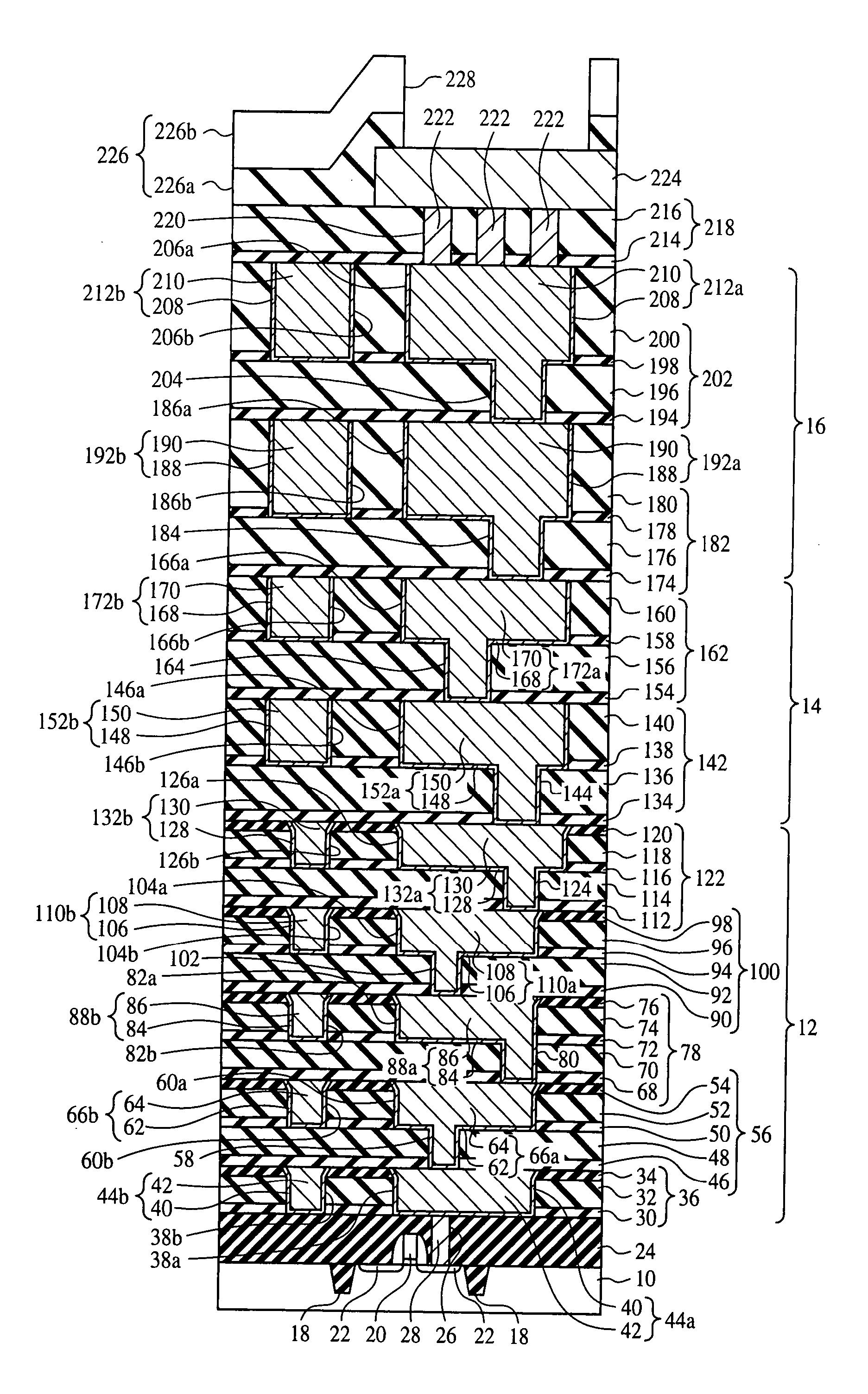
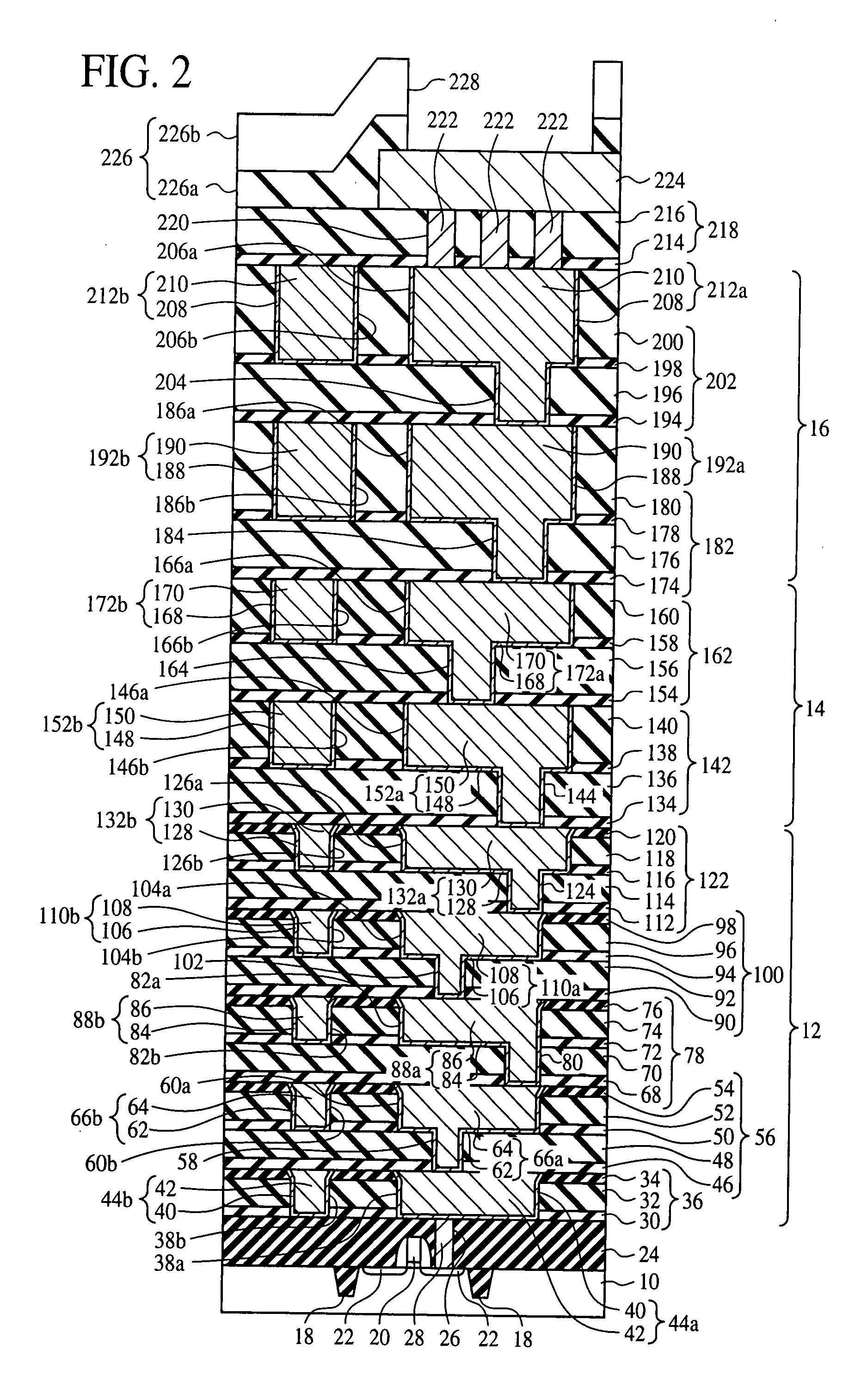
[0050] In order to decrease the interconnection capacitance of semiconductor devices, as described above, the use of low-k materials as materials of the inter-layer insulation films is being studies. As the low-k materials are known SiOC, SILK (registered trademark) by The Dow Chemical Company, FLARE (registered trademark) by Honeywell Electronic Materials, etc. Most of such low-k materials are water-repellent. This is for the following reason. The relative dielectric constant of water is as high as 88. Accordingly, when a film formed of a low-k material absorbs humidity, the dielectric constant of the film rises. To suppress the dielectric constant increase due to the humidity absorption, the low-k materials are terminated with Si—H, SiCH3 for the processing for prohibiting the formation of Si—OH bonds, which are hydrophilic.

[0051] As mentioned above, in order to suppress the dielectric constant increase due to the humidity absorption, the low-k materials are terminated with hydro...


PUM


Abstract

The semiconductor device comprises a lower interconnection part 12 which is formed on a silicon substrate 10 and includes an inter-layer insulation film 36 formed of a low-k film 32 and a hydrophilic insulation film 34 formed on the low-k film 32, and an interconnection layer 44a, 44b buried in interconnection trenches 38a, 38b formed in the inter-layer insulation film 36 and having an interconnection pitch which is a first pitch; and an intermediate interconnection part 14 which is formed on the lower interconnection part 12 and includes an inter-layer insulation film 142 formed of low-k films 136, 140, an interconnection layer 152a, 152b buried in interconnection trenches 146a, 146b formed in the inter-layer insulation film 142 and having an interconnection pitch which is a second pitch larger than the first pitch, and an SiC film 154 formed directly on the low-k film 140 and the interconnection layer 152a, 152b.

Description

CROSS-REFERENCE TO RELATED APPLICATION [0001] This application is a divisional of Ser. No. 10 / 816,955, filed on Apr. 5, 2004, which is based upon and claims priority of Japanese Patent Application No. 2003-372304, filed on Oct. 31, 2003, the contents being incorporated herein by reference.BACKGROUND OF THE INVENTION [0002] The present invention relates to a semiconductor device having a multilayer interconnection structure and a method for fabricating the semiconductor device, more specifically a semiconductor device having a multilayer interconnection structure using low dielectric constant (low-k) films as the inter-layer insulation films and a method for fabricating the semiconductor device. [0003] The recent increasing micronization of semiconductor devices requires decrease of the interconnection resistance and interconnection capacitance of the semiconductor devices. [0004] To meet such requirement, the main material of the interconnections is shifting from Al (aluminum) to Cu...

Claims


Application Information

Patent Timeline
Patent Type & Authority Applications(United States)
IPC IPC(8): H01L21/3205H01L21/768H01L23/053H01L23/485H01L23/532
CPCH01L21/76808H01L21/76829H01L2924/13091H01L2224/02166H01L2924/0002H01L2924/01072H01L2924/01033H01L2924/01019H01L2924/30105H01L21/76838H01L23/53238H01L23/53295H01L24/03H01L24/05H01L2224/05093H01L2224/05096H01L2224/05556H01L2224/05567H01L2224/05624H01L2924/01004H01L2924/01005H01L2924/01006H01L2924/01013H01L2924/01014H01L2924/01018H01L2924/01022H01L2924/01027H01L2924/01029H01L2924/0105H01L2924/01073H01L2924/01074H01L2924/01078H01L2924/04941H01L2924/04953H01L2924/05042H01L2924/00014H01L2924/00H01L2224/05552
Inventor OTSUKA, SATOSHI
Owner FUJITSU MICROELECTRONICS LTD
Why Eureka
Try Eureka