Bottom gate thin film transistor and method of manufacturing the same

bottom gate technology, applied in the field of manufacturing a thin film transistor, can solve the problems of increasing manufacturing costs, and achieve the effect of simple and easy manufacturing of improved field effect mobility

Inactive Publication Date: 2007-12-13
SAMSUNG ELECTRONICS CO LTD
View PDF5 Cites 27 Cited by
  • Summary
  • Abstract
  • Description
  • Claims
  • Application Information

AI Technical Summary

Benefits of technology

[0011]According to exemplary embodiments of the present invention, a bottom gate TFT having improved field effect mobility can be manufactured simply and easily.

Problems solved by technology

The additional operation is not desirable in view of mass production, and in particular, may affect product yield, thus resulting in increased manufacturing costs.

Method used


Image

  • Bottom gate thin film transistor and method of manufacturing the same
  • Bottom gate thin film transistor and method of manufacturing the same
  • Bottom gate thin film transistor and method of manufacturing the same

Examples


Embodiment Construction

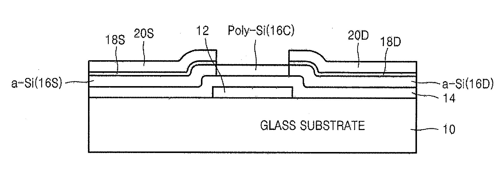
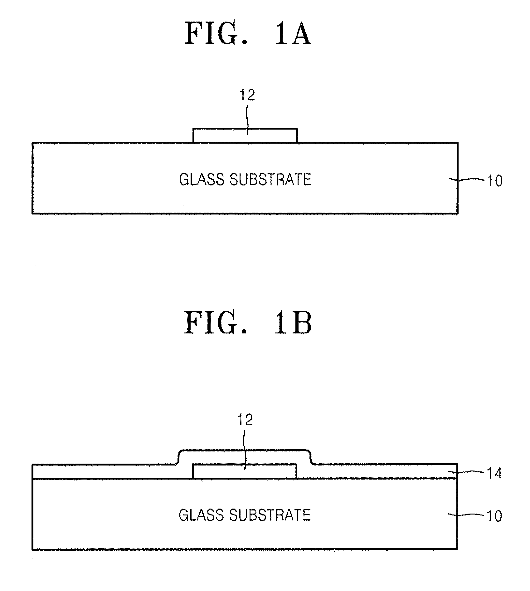
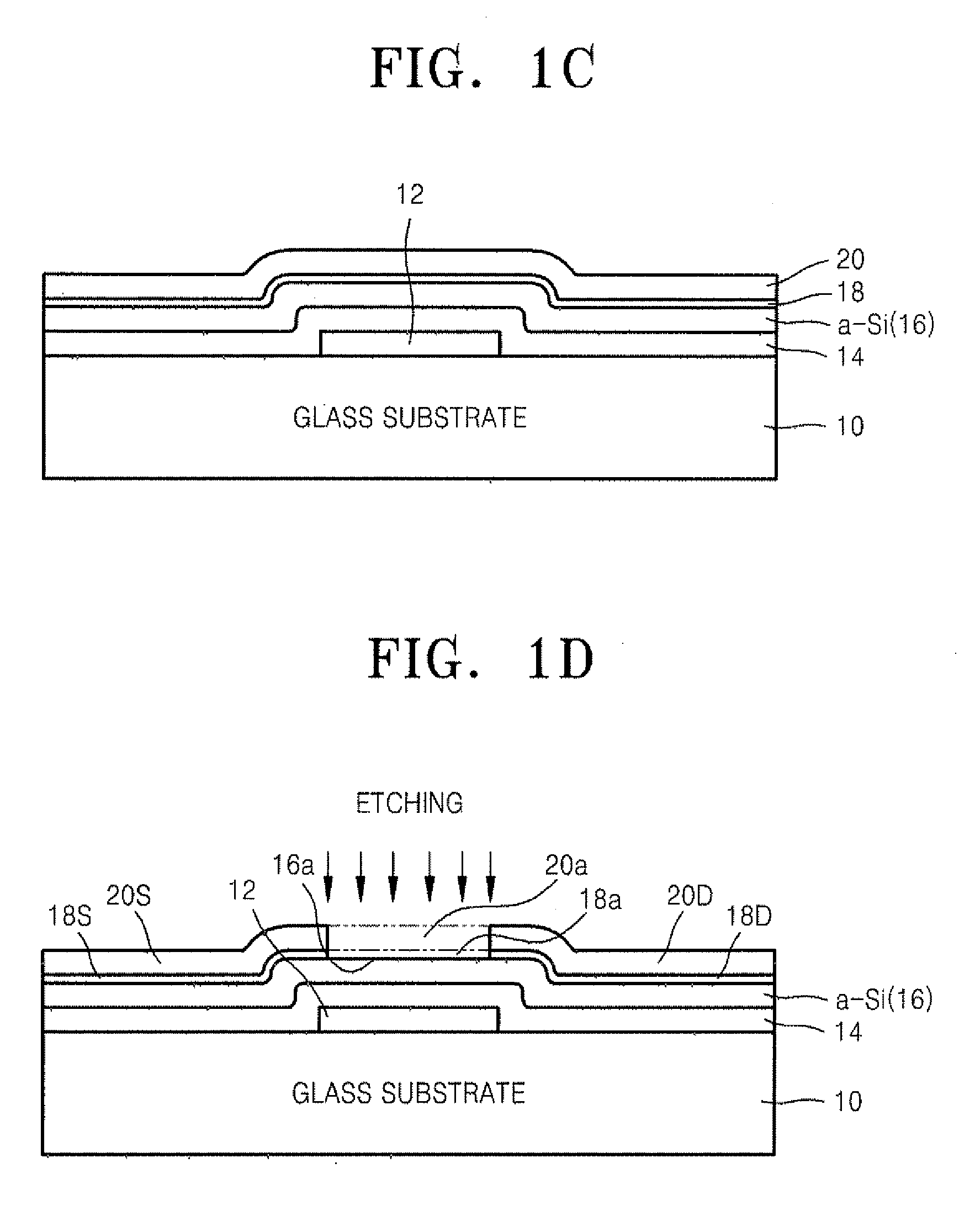
[0015]The present invention will now be described more fully hereinafter with reference to the accompanying drawings, in which exemplary embodiments of the present invention are shown. This invention may, however, be embodied in many different forms and should not be construed as limited to the exemplary embodiments set forth herein. Rather, these exemplary embodiments are provided so that this disclosure will be thorough and complete, and will fully convey the scope of the invention to those skilled in the art. Like reference numerals refer to like elements throughout.

[0016]It will be understood that, although the terms first, second, third etc. may be used herein to describe various elements, components, regions, layers and / or sections, these elements, components, regions, layers and / or sections should not be limited by these terms. These terms are only used to distinguish one element, component, region, layer or section from another element, component, region, layer or section. T...


PUM


Abstract

A method of manufacturing a bottom gate thin film transistor (“TFT”) in which a polycrystalline channel region having a large grain size is formed relatively simply and easily. The method of manufacturing a bottom gate thin film transistor includes forming a bottom gate electrode on a substrate, forming a gate insulating layer on the substrate to cover the bottom gate electrode, forming an amorphous semiconductor layer, an N-type semiconductor layer and an electrode layer on the gate insulating layer sequentially, etching an electrode region and an N-type semiconductor layer region formed on the bottom gate electrode sequentially to expose an amorphous semiconductor layer region, melting the amorphous semiconductor layer region using a laser annealing method, and crystallizing the melted amorphous semiconductor layer region to form a laterally grown polycrystalline channel region.

Description

[0001]This application claims priority to Korean Patent Application No. 10-2006-0052101, filed on Jun. 9, 2006, and all the benefits accruing therefrom under 35 U.S.C. §119, the contents of which in its entirety are herein incorporated by reference.BACKGROUND OF THE INVENTION[0002]1. Field of the Invention[0003]The present invention relates to a method of manufacturing a thin film transistor (“TFT”), and more particularly, to a method of manufacturing a bottom gate TFT in which a polycrystalline channel region having a large grain size can be formed relatively simply and easily.[0004]2. Description of the Related Art[0005]Active research on a low temperature poly-Si (“LTPS”) TFT, which is used in light sources of organic light emitting display (“OLED”) devices or liquid crystal display (“LCD”) devices, has been conducted recently. Accordingly, research on a system on glass (“SOG”), in which an outer driver integrated circuit (“IC”) is never employed, has been further conducted. The ...

Claims


Application Information

Patent Timeline
Patent Type & Authority Applications(United States)
IPC IPC(8): H01L29/76H01L29/10
CPCH01L21/268H01L29/66765H01L29/78609H01L27/1285H01L29/78684H01L29/78696H01L29/78678H01L21/02675
Inventor LIM, HYUCKPARK, YOUNG-SOOXIANYU, WENXUCHA, YOUNG-KWAN
Owner SAMSUNG ELECTRONICS CO LTD
Why Eureka
Try Eureka