Nitride-based semiconductor light emitting diode

a light-emitting diode and nitride-based technology, applied in the direction of semiconductor devices, basic electric elements, electrical appliances, etc., can solve the problems of reducing the reliability and production yield of nitride-based semiconductor leds, and achieve the effects of minimizing esd impact, maximizing current spreading effect, and wide width

Inactive Publication Date: 2007-12-13
SAMSUNG ELECTRO MECHANICS CO LTD
View PDF2 Cites 24 Cited by
  • Summary
  • Abstract
  • Description
  • Claims
  • Application Information

AI Technical Summary

Benefits of technology

[0018] An advantage of the present invention is that it provides a high-luminance nitride-based semiconductor LED which can optimize a current spreading effect, and simultaneously, minimize ESD impact, thereby stabilizing a characteristic thereof from high static electricity.
[0019] Additional aspect and advantages of the present general inventive concept will be set forth in part in the description which follows and, in part, will be obvious from the description, or may be learned by practice of the general inventive concept.
[0020] According to an aspect of the invention, a nitride-based semiconductor LED comprises a substrate; an n-type nitride semiconductor layer formed on the substrate; an active layer formed on a predetermined region of the n-type nitride semiconductor layer; a p-type nitride semiconductor layer formed on the active layer; a p-electrode formed on the p-type nitride semiconductor layer, the p-electrode having a p-type branch electrode; a p-type ESD pad formed at the end of the p-type branch electrode, the p-type ESD pad having a larger width than the end of the p-type branch electrode; an n-electrode formed on the n-type nitride semiconductor layer, on which the active layer is not formed, the n-electrode having an n-type branch electrode; and an n-type ESD pad formed at the end of the n-type branch electrode, the n-type ESD pad having a larger width than the end of the n-type branch electrode.
[0021] According to another aspect of the invention, the n-type and p-type branch electrodes, respectively, are composed of one or more lines, the line being selected from a group consisting of a straight line, a curved line, and a looped line.
[0022] According to a further aspect of the invention, the n-type and p-type branch electrodes are formed so as to extend from the n-electrode and the p-electrode, respectively, in one direction.
[0023] According to a still further aspect of the invention, the n-electrode and the p-electrode are formed in a shape selected from a group consisting of a circular shape, a polygonal shape, and another polygonal shape of which the corner is formed in a curved line.

Problems solved by technology

As a result, such a structure acts as a main cause which unstabilizes a characteristic of the nitride-based semiconductor LED, thereby reducing the reliability and production yield of the nitride-based semiconductor LED.

Method used


Image

  • Nitride-based semiconductor light emitting diode
  • Nitride-based semiconductor light emitting diode
  • Nitride-based semiconductor light emitting diode

Examples


first embodiment

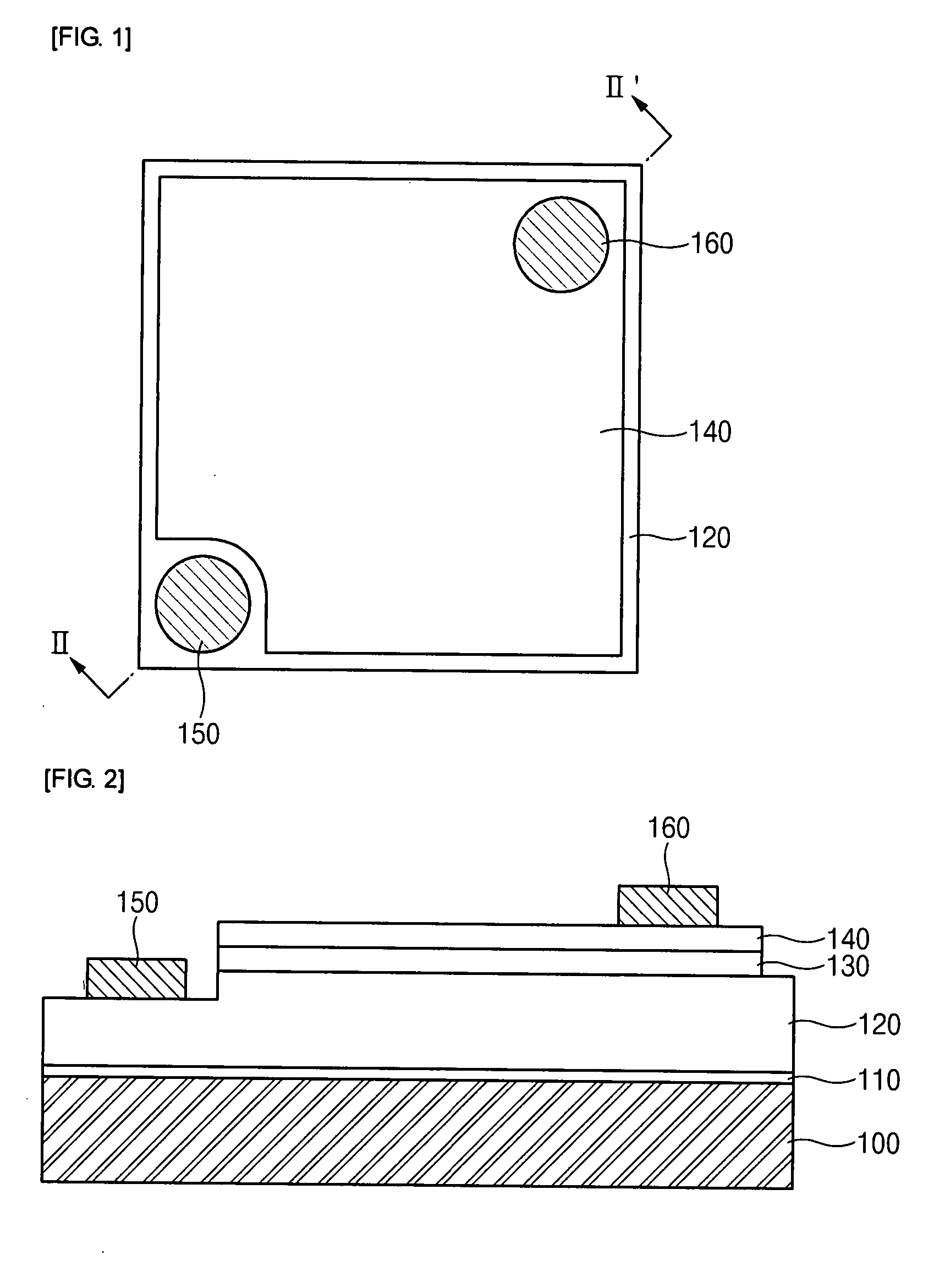
[0039] First, a nitride-based semiconductor LED according to a first embodiment of the invention will be described with reference to FIGS. 4 and 5.

[0040]FIG. 4 is a plan view illustrating the structure of the nitride-based semiconductor LED according to the first embodiment of the invention, and FIG. 5 is a sectional view taken along IV-IV′ line of FIG. 4.

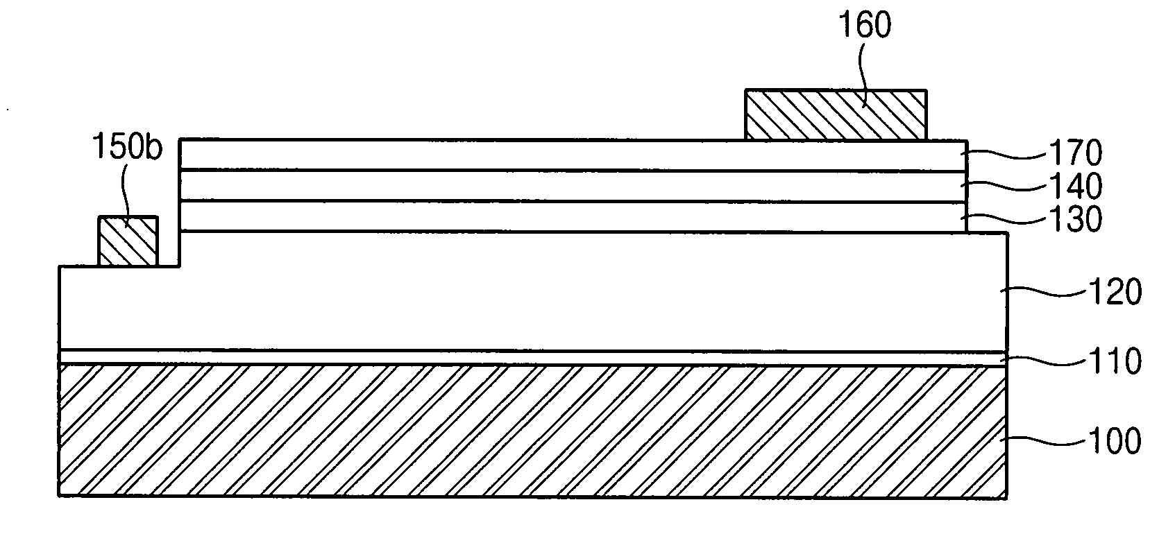
[0041] As shown in FIGS. 4 and 5, the nitride-based semiconductor LED according to the first embodiment of the invention includes an optically-transparent substrate 100 and a light-emitting structure in which a buffer layer 110, an n-type nitride semiconductor layer 120, an active layer 130, and a p-type nitride semiconductor layer 140 are sequentially laminated on the substrate 100.

[0042] The substrate 100 may be a heterogeneous substrate, such as a sapphire substrate and a silicon carbide (SiC) substrate, or a homogeneous substrate such as a nitride substrate, which is suitable for growing nitride semiconductor single crystal....

second embodiment

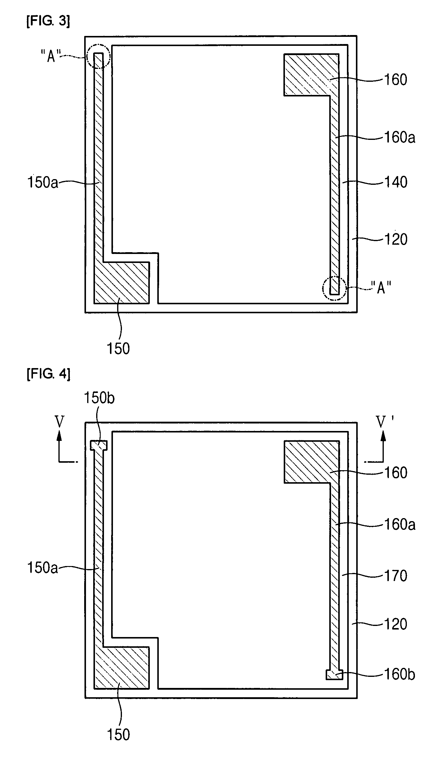
[0058] Now, a nitride-based semiconductor LED according to a second embodiment of the invention will be described in detail with reference to FIG. 7. However, the descriptions of the same components of the second embodiment as those of the first embodiment will be omitted.

[0059]FIG. 7 is a plan view illustrating the structure of the nitride-based semiconductor LED according to the second embodiment.

[0060] As shown in FIG. 7, the nitride-based semiconductor LED according to the second embodiment has almost the same construction as the nitride-based semiconductor LED according to the first embodiment. In the second embodiment, however, an n-type electrode 150 and a p-type electrode 160 are formed in a hemispherical shape, not a rectangular shape. Further, two p-type branch electrodes 160a are disposed in a finger shape such that the p-type branch electrodes 160a are parallel to each other.

[0061] Similar to the first embodiment, n-type and p-type ESD pads 150b and 160b are formed at...


PUM


Abstract

A nitride-based semiconductor LED comprises a substrate; an n-type nitride semiconductor layer formed on the substrate; an active layer formed on a predetermined region of the n-type nitride semiconductor layer; a p-type nitride semiconductor layer formed on the active layer; a p-electrode formed on the p-type nitride semiconductor layer, the p-electrode having a p-type branch electrode; a p-type ESD pad formed at the end of the p-type branch electrode, the p-type ESD pad having a larger width than the end of the p-type branch electrode; an n-electrode formed on the n-type nitride semiconductor layer, on which the active layer is not formed, the n-electrode having an n-type branch electrode; and an n-type ESD pad formed at the end of the n-type branch electrode, the n-type ESD pad having a larger width than the end of the n-type branch electrode.

Description

CROSS-REFERENCE TO RELATED APPLICATIONS [0001] This application claims the benefit of Korean Patent Application No. 10-2006-0043986 filed with the Korean Intellectual Property Office on May 16, 2006, the disclosure of which is incorporated herein by reference. BACKGROUND OF THE INVENTION [0002] 1. Field of the Invention [0003] The present invention relates to a nitride-based semiconductor light emitting diode in which a p-electrode and an n-electrode having high resistance to electrostatic discharge (hereinafter, referred to as ESD) have a lateral structure. [0004] 2. Description of the Related Art [0005] In general, light emitting diodes (hereinafter, referred to as LEDs) are semiconductor elements which convert an electrical signal into infrared rays, visible rays, or light by using a characteristic of compound semiconductor, i.e., a recombination of electrons and holes, in order to send and receive signals. [0006] LEDs are generally used in home appliances, remote controls, elect...

Claims


Application Information

Patent Timeline
Patent Type & Authority Applications(United States)
IPC IPC(8): H01L33/00H01L31/12H01L27/15H01L29/26H01L33/32H01L33/38H01L33/42
CPCH01L33/38H01L33/20
Inventor KO, KUN YOOOH, BANG WONHWANG, SEOK MINKIM, JE WONPARK, HYUNG JINKIM, DONG WOO
Owner SAMSUNG ELECTRO MECHANICS CO LTD
Why Eureka
Try Eureka