

Electrostatic discharge protection method and device for semiconductor device
a technology of electrostatic discharge and protection method, which is applied in the direction of variable capacitors, fixed capacitors, instruments, etc., can solve the problems of insufficient protection of internal circuits, internal circuit breakage, and terminal voltage increase, so as to prevent the expansion of the layout area, and increase the breakdown voltage at the pn junction between the emitter terminal and the base terminal.
- Summary
- Abstract
- Description
- Claims
- Application Information
AI Technical Summary
Benefits of technology
Problems solved by technology
Method used
Image

Examples
first embodiment
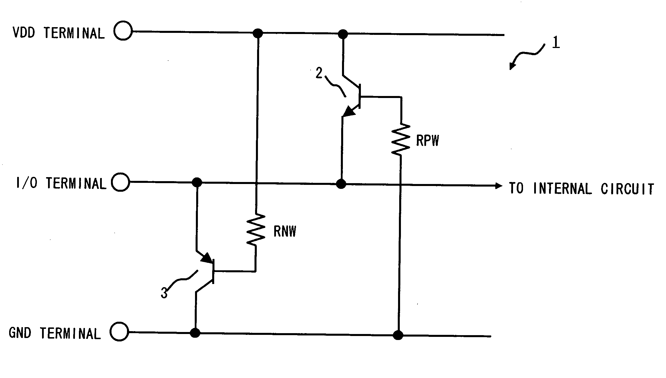
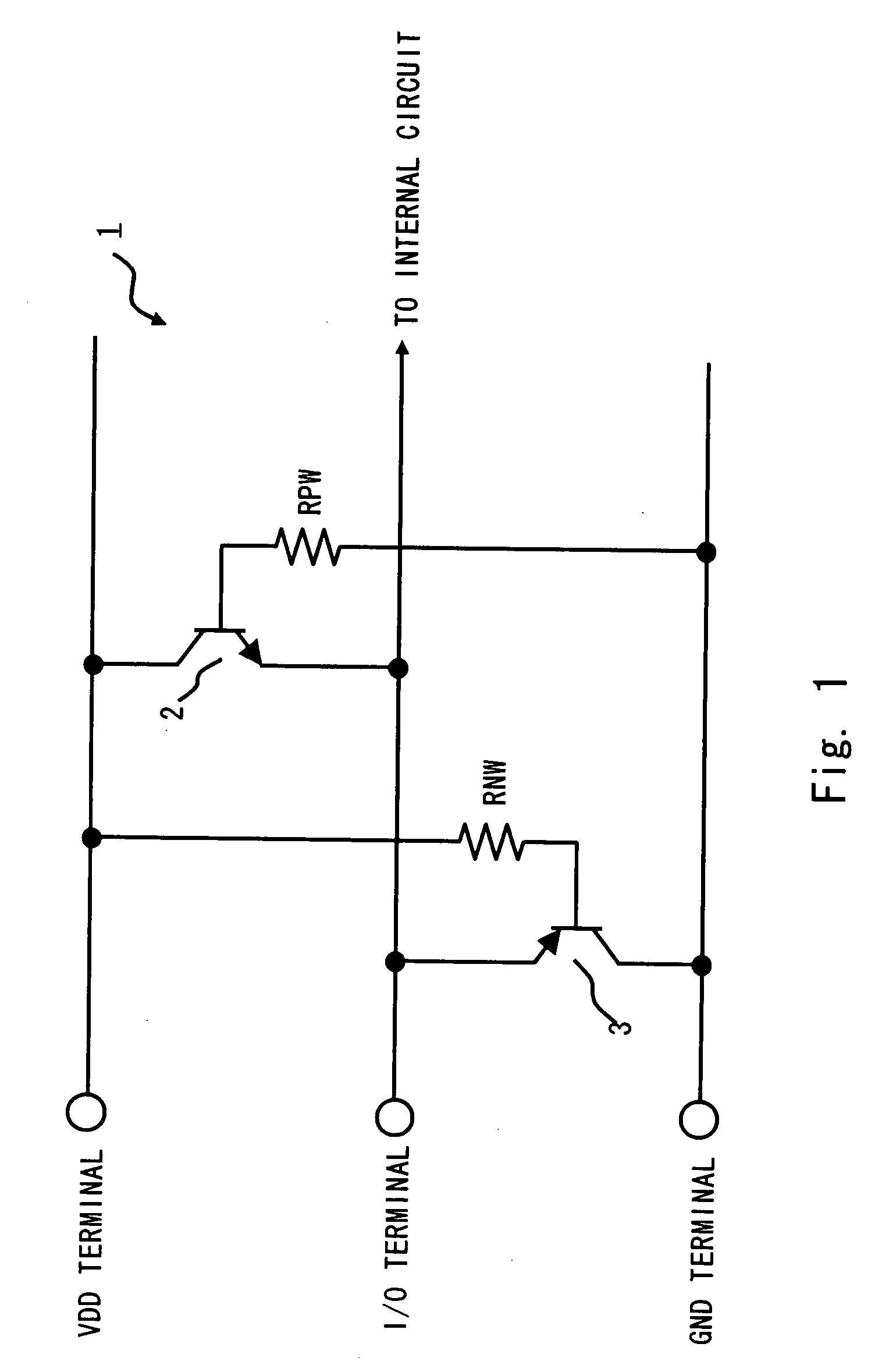
[0047]Hereinafter, embodiments of the present invention are described with reference to the accompanying drawings. FIG. 1 is a circuit diagram of an electrostatic discharge protection device 1 according to a first embodiment of the present invention. As shown in FIG. 1, the electrostatic discharge protection device 1 of the first embodiment includes a first bipolar transistor (for example, NPN transistor 2) and a second bipolar transistor (for example, PNP transistor 3). Further, the electrostatic discharge protection device 1 includes a first power supply terminal (for example, power supply terminal; hereinafter referred to as “VDD terminal”), an input / output terminal (hereinafter referred to as “I / O terminal”), and a second power supply terminal (for example, ground terminal; hereinafter referred to as “GND terminal”). The I / O terminal is connected with an internal circuit of the semiconductor device. The internal circuit is a circuit including an NMOS transistor and a PMOS transi...
second embodiment
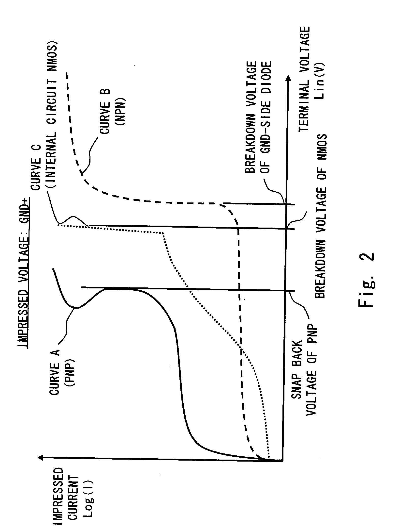
[0084]A electrostatic discharge protection device 1a according to a second embodiment of the present invention differs from the electrostatic discharge protection device 1 of the first embodiment in that a resistance value of the parasitic resistance (resistor RNW and resistor RPW) formed in the well region is substantially increased. If a resistance value of the parasitic resistance is increased, after the breakdown of a diode between the emitter terminal and the base terminal, a potential difference between the I / O terminal and the VDD terminal or GND terminal can be increased in accordance with an amount of surge current. By increasing the potential difference, even if a breakdown operation of the diode precedes the snap back operation of the transistor, the transistor starts the snap back operation before the diode is broken down.
[0085]For example, if a breakdown voltage of the diode largely fluctuates due to variations in manufacturing step, it is effective to substantially inc...
PUM
 Abstract
Description
Claims
Application Information