
Semiconductor device

a technology of semiconductor devices and semiconductors, applied in semiconductor devices, digital storage, instruments, etc., can solve the problems of high-speed writing not being performed, and erroneous writing at reading

Inactive Publication Date: 2007-12-13
HITACHI LTD
View PDF4 Cites 32 Cited by
  • Summary
  • Abstract
  • Description
  • Claims
  • Application Information

AI Technical Summary

Benefits of technology

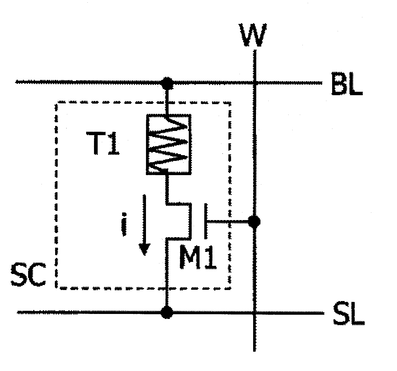
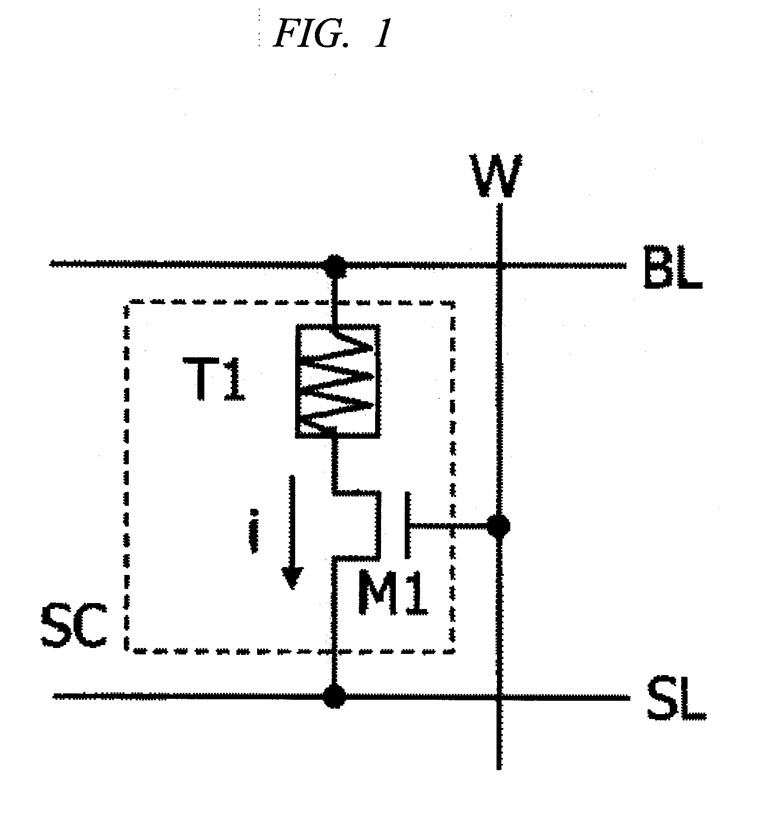
[0006]Further, a spin-injection MRAM is excellent in scalability and it can be miniaturized. However, according to advance of miniaturization, manufacture variations among respective memory cells become large, so that variations in write current may occur among the respective memory cells. Therefore, it is necessary to reduce variations among currents caused to flow in memory cells at writing.

Problems solved by technology

On the contrary, when a small MOS transistor is used in order to reduce an area, high-speed writing can not be performed.
However, according to advance of miniaturization, manufacture variations among respective memory cells become large, so that variations in write current may occur among the respective memory cells.
Therefore, such a possibility occurs that erroneous write may be conducted at reading.

Method used


Image

  • Semiconductor device
  • Semiconductor device
  • Semiconductor device

Examples


second embodiment

[0064]the present invention will be explained with reference to FIG. 12. Currents flowing in a memory cell at times of read operation and write operation and pulse widths of the currents are observed. A feature of the present invention lies in that current amounts for read and write are approximately equal to each other and the pulse width at the read operation time is smaller than the pulse width at the write operation time. More specifically, the current value is i4 and the same in both the times, but when the pulse width t5 at the read time is compared with the pulse width t6 at the write time, t5 is smaller than t6. When the feature is compared with flash memory, write current is smaller than read current for each memory cell and a required pulse width at the write time is larger than that at the read time, for example, in NAND flash memory. In MRAM which causes a wire to generate magnetic field utilizing current to perform rewrite, current at the write time is large. The readin...

third embodiment

[0069]FIG. 17 is a diagram showing the present invention. In this embodiment, in order to apply a potential to the bit line BL, a capacitor CS, a switch S1 for connecting the capacitor CS to a power supply Vd, and a switch S2 for connecting the capacitor CS to the bit line BL are prepared. Conventionally, in order to supply a potential to the bit line BL, a configuration where the power supply Vd and the bit line BL are connected by a switch has been adopted. When the bit line is directly connected to the power supply like this manner, such a case may occur where flowing currents are different among respective memory cells due to performances of MOS transistors constituting the memory cells. In this embodiment, unlike the abovementioned case, the switch S1 is first closed so that the capacitor CS is charged by the power supply Vd. Thereafter, the switch S1 is opened and the switch S2 is closed so that current is supplied to the bit line BL with charge of the capacitor CS. By using t...

fourth embodiment

[0076]FIG. 26 is a diagram of a layout example of a memory cell array showing the present invention. FIG. 26 shows only a portion corresponding to FIG. 24. A feature of the embodiment lies in that an assist word line AW running in parallel with the word line is disposed below the bottom electrode BE. By causing current to flow in the assist word line AW, a magnetic field can be generated, so that it can influence the operation of the TMR device.

[0077]FIG. 27 is circuit diagrams corresponding to the memory cell of the sectional structure shown in FIG. 26. The word line W and the assist word line AW are arranged in parallel, and it is indicated by an arrow that the assist word line AW can influence the TMR device T1 by the magnetic field generated by current flowing in the assist word line. As the operation example, there are examples shown by FIG. 27A and FIG. 27B. More specifically, only the assist word line is first turned ON to cause current to flow, as shown in FIG. 27A. Therefor...


PUM


Abstract

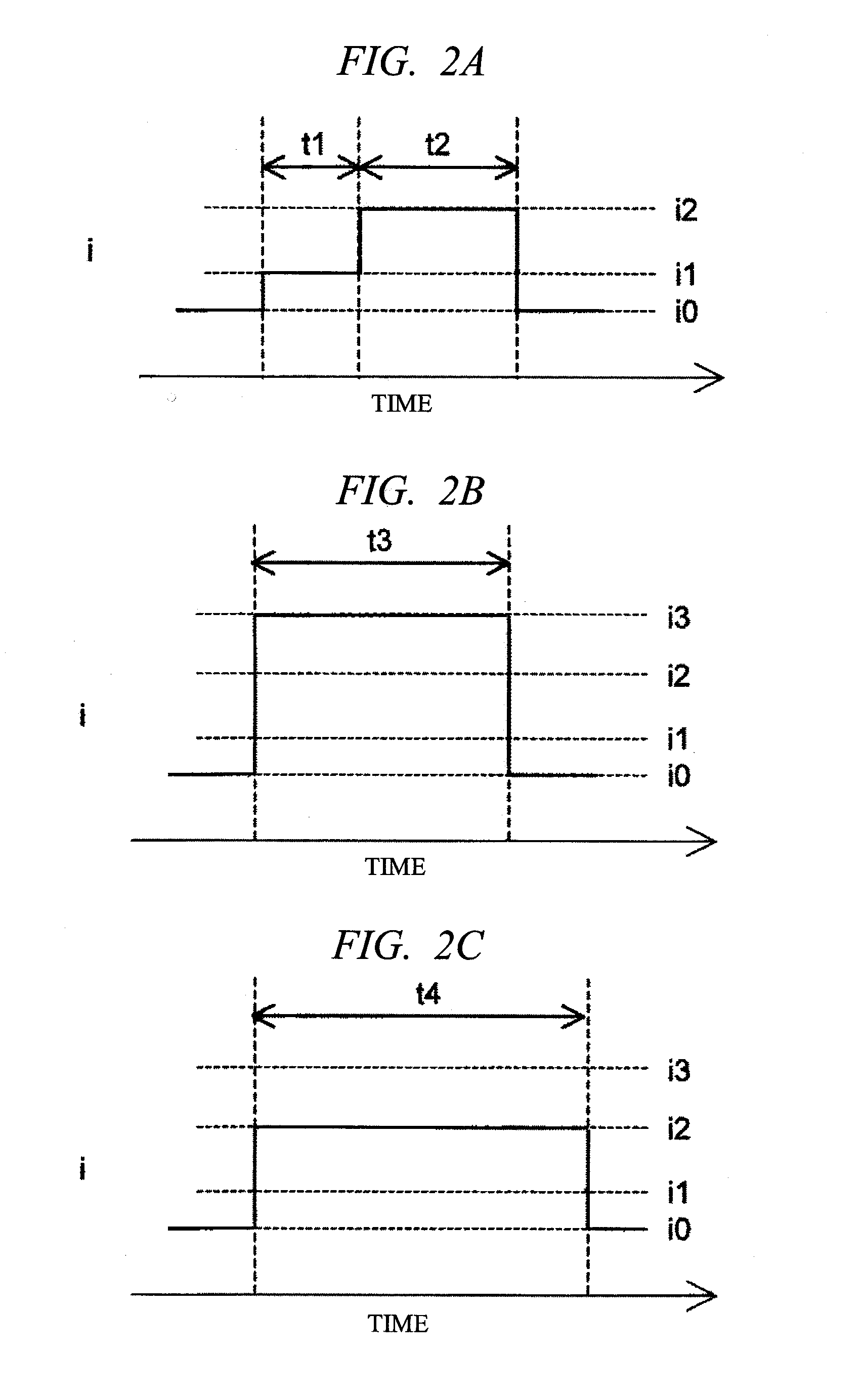
In a memory using spin transfer torque, state of the spin is made unstable by applying a weak pulse before rewriting to reduce rewrite current. Reading of high-speed operation is performed with current in a regime where the current becomes non-linearly increases corresponding to the pulse width to suppress disturb. Further, fluctuation of respective memory cells is suppressed by a driving method setting the amount of spin constant by bit line charge to suppress read disturb.

Description

CROSS-REFERENCE TO RELATED APPLICATION[0001]The present application claims priority from Japanese Patent Application No. JP 2006-138429 filed on May 18, 2006, the content of which is hereby incorporated by reference into this application.TECHNICAL FIELD OF THE INVENTION[0002]The present invention relates to a semiconductor device, and in particular, to a method for controlling writing to a memory cell utilizing magnetoresistive change.BACKGROUND OF THE INVENTION[0003]Of non-volatile memories, MRAM (magnetoresistive random access memory) utilizing magnetoresistance change has a possibility that it serves as RAM capable of high-speed operation. A cell arrangement of a conventional MRAM is composed of one tunneling magnetoresistance TMR and a select transistor MCT for read operation, a write word line WWL and a bit line BL, and a source line SL. As shown in FIG. 30, the tunneling magnetoresistance TMR includes at least two magnetic layers, one thereof being a fixed layer PL where a dir...

Claims


Application Information

Patent Timeline
IPC IPC(8): G11C11/02
CPCH01L27/228G11C11/16G11C11/1659G11C11/1673G11C11/1675G11C11/1653G11C11/1693G11C11/1657H10B61/22G11C11/15H10N50/10
Inventor KAWAHARA, TAKAYUKITAKEMURA, RIICHIROITO, KENCHITAKAHASHI, HIROMASA
Owner HITACHI LTD
Learn More