Surface mounting structure and packaging method thereof

a surface mounting and structure technology, applied in semiconductor devices, semiconductor/solid-state device details, electrical apparatus, etc., can solve problems such as the development of tiny electronic products, and achieve the effects of simplifying system design, increasing space utilization rate, and increasing use spa

Inactive Publication Date: 2007-12-20
LITE ON SEMICON
View PDF2 Cites 101 Cited by
  • Summary
  • Abstract
  • Description
  • Claims
  • Application Information

AI Technical Summary

Benefits of technology

[0007]It is a primary object of the present invention to provide a surface mounting structure and a packaging method thereof in which two conducting wires instead of lead frame architecture of the prior art is that the lead frame and a bridge jumper connected with N junction and P junction instead of the conduc...

Problems solved by technology

Furthermore, the traditional SMD package is that lead frames are used and pins are drawn out from two sides of the package to cause larger occupation volume s...

Method used


Image

  • Surface mounting structure and packaging method thereof
  • Surface mounting structure and packaging method thereof
  • Surface mounting structure and packaging method thereof

Examples


Embodiment Construction

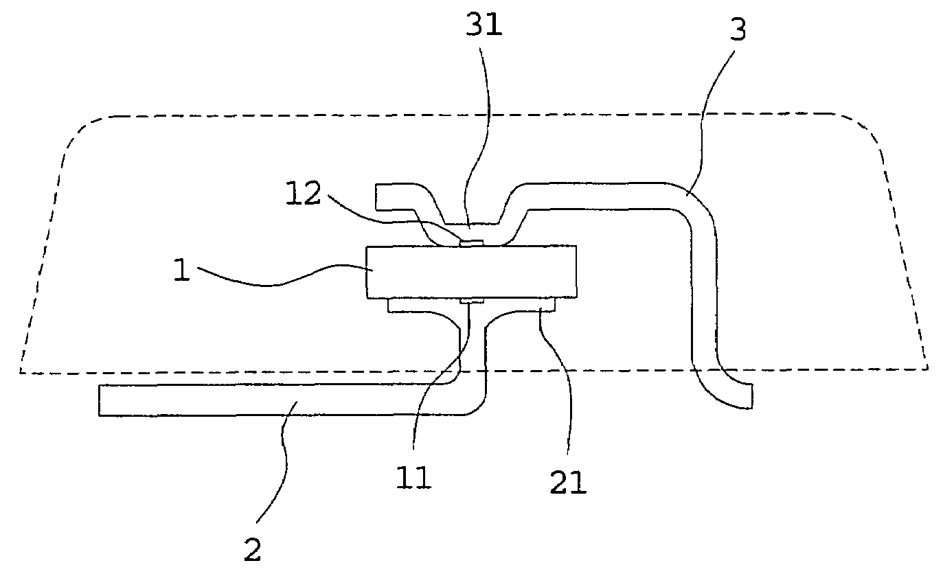
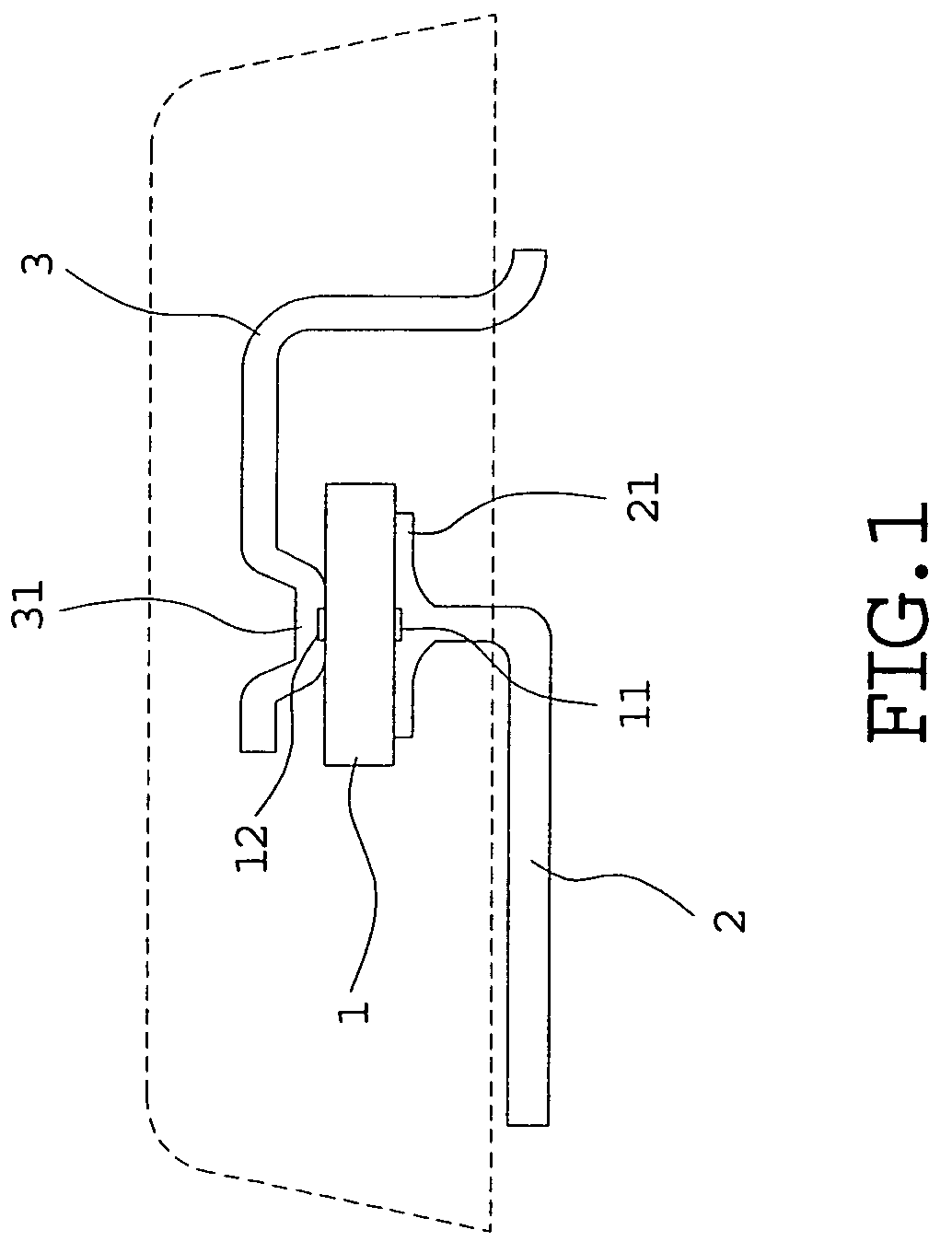
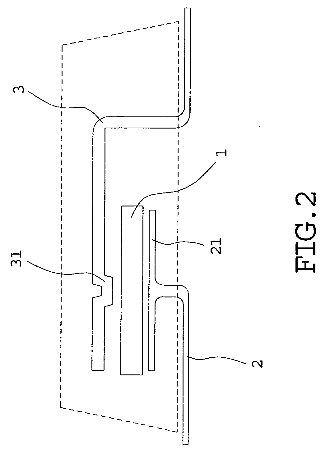
[0019]References are made from FIG. 1 to FIG. 3 which are three schematic views of a surface mounting structure and a packaging method thereof of the present invention. The surface mounting structure comprises a chip 1, a first conducting wire 2 and a second conducting wire 3. The chip 1 has a first electrode 11 and a second electrode 12. A front end of the first conducting wire 2 has a supporting portion 21 for supporting the chip 1. The second conducting wire 3 is connected with one end of the chip 1, and the first electrode 11 is electrically connected with the first conducting wire 2 and the second electrode 12 is electrically connected with the second conducting wire 3.

[0020]The supporting portion 21 of the first conducting wire 2 is a flat shape (similar to a platform) by means of a stretching and pressing process, the flat-shaped supporting portion 21 is horizontal to an upper flat surface and a lower flat surface of a housing for supporting the chip 1. A rear end of the firs...


PUM


Abstract

A surface mounting structure and a packaging method thereof comprises a chip, a first conducting wire and a second conducting wire. The two conducting wires instead of lead frame architecture of the prior art is that the lead frame and a bridge jumper connected with N junction and P junction instead of the two conducting wires. The two conducting wires are drawn out from a bottom of a package, and are pressed and bent to original surface of the surface mounting pins so as to increase space utilization rate. Thereby it is to improve a complicated lead frame architecture of the prior art, increase use space and simplify system design.

Description

BACKGROUND OF THE INVENTION[0001]1. Field of the invention[0002]The present invention relates to a surface mounting device, and more particularly to a surface mounting structure of two conducting wires and a packaging method thereof.[0003]2. Description of the Prior Art[0004]Recently with the rapidly development of manufacturing skills of the integrated circuit, the tinny dimensions of the electronic elements have become a necessary trend, and larger scale and higher integration of the electronic circuit so as to produce more complete productions. In this condition, the traditional assembly way of pin through hole (PTH) needs larger space of the printed circuit board to insert elements, and one side of the printed circuit board is used to insert pins of the elements and the other side is used to weld pins of the elements. Hence, a packaging method of surface mounting device (SMD) is used to assemble the electronic components on the printed circuit board at present.[0005]Furthermore,...

Claims


Application Information

Patent Timeline
IPC IPC(8): H01L23/48H01L21/44
CPCH01L23/49562H01L24/01H01L24/80H01L2924/01033H01L2924/01082H01L2924/14H01L2924/01015
Inventor WU, KUO-LIANGIU, KUO-SHUCHANG, CHIH-WEI
Owner LITE ON SEMICON
Why Eureka
Try Eureka