Electronic component, semiconductor device employing same, and method for manufacturing electronic component

a semiconductor device and electronic component technology, applied in the field of electronic components, can solve the problems of increasing the mounting area and cost, lowering the yield, and increasing the bonding strength between the bump electrode and the semiconductor substrate, so as to reduce the area of the underlying metal layer formed under the external connection electrode, reduce the bonding area, and reduce the bonding strength

Active Publication Date: 2007-12-20
SONY CORP
View PDF2 Cites 87 Cited by
  • Summary
  • Abstract
  • Description
  • Claims
  • Application Information

AI Technical Summary

Benefits of technology

[0052]In the electronic component according to the embodiment of the present invention, the underlying metal layer is formed on the recess or/and the projection provided under the barrier metal layer outside or/and inside the opening, so that the underlying metal layer has a surface shape that follows the recess or/and the projection. Thus, the area of the underlying metal layer formed under the external connection electrode can be increased. This can prevent the lowering of the bonding strength between the external connection electrode and the substrate attributed to decrease in the bonding area between the barrier metal layer and the underlying metal layer, arising due to side etching (undercut) at the time of removal of the unnecessary part of the underlying metal layer by wet etching. Consequently, an electronic component having an external connection electrode that allows highly reliable electric connection can be provided.
[0053]Furthermore, the semiconductor device employing the electronic component according to the embodiment of the present invention is externally connected to the electronic component via the external connection electrode. This can provid...

Problems solved by technology

Along with enhancement of the integration degree and performance of LSIs, the chip size is ever-increasing, which leads to serious problems such as the lowering of the yield and increases in the mounting area and costs.
This decreases the bonding area between the barrier metal layer and the underlying metal layer, which lowers the bonding strength between the bump electrode and...

Method used


Image

  • Electronic component, semiconductor device employing same, and method for manufacturing electronic component
  • Electronic component, semiconductor device employing same, and method for manufacturing electronic component
  • Electronic component, semiconductor device employing same, and method for manufacturing electronic component

Examples


first embodiment

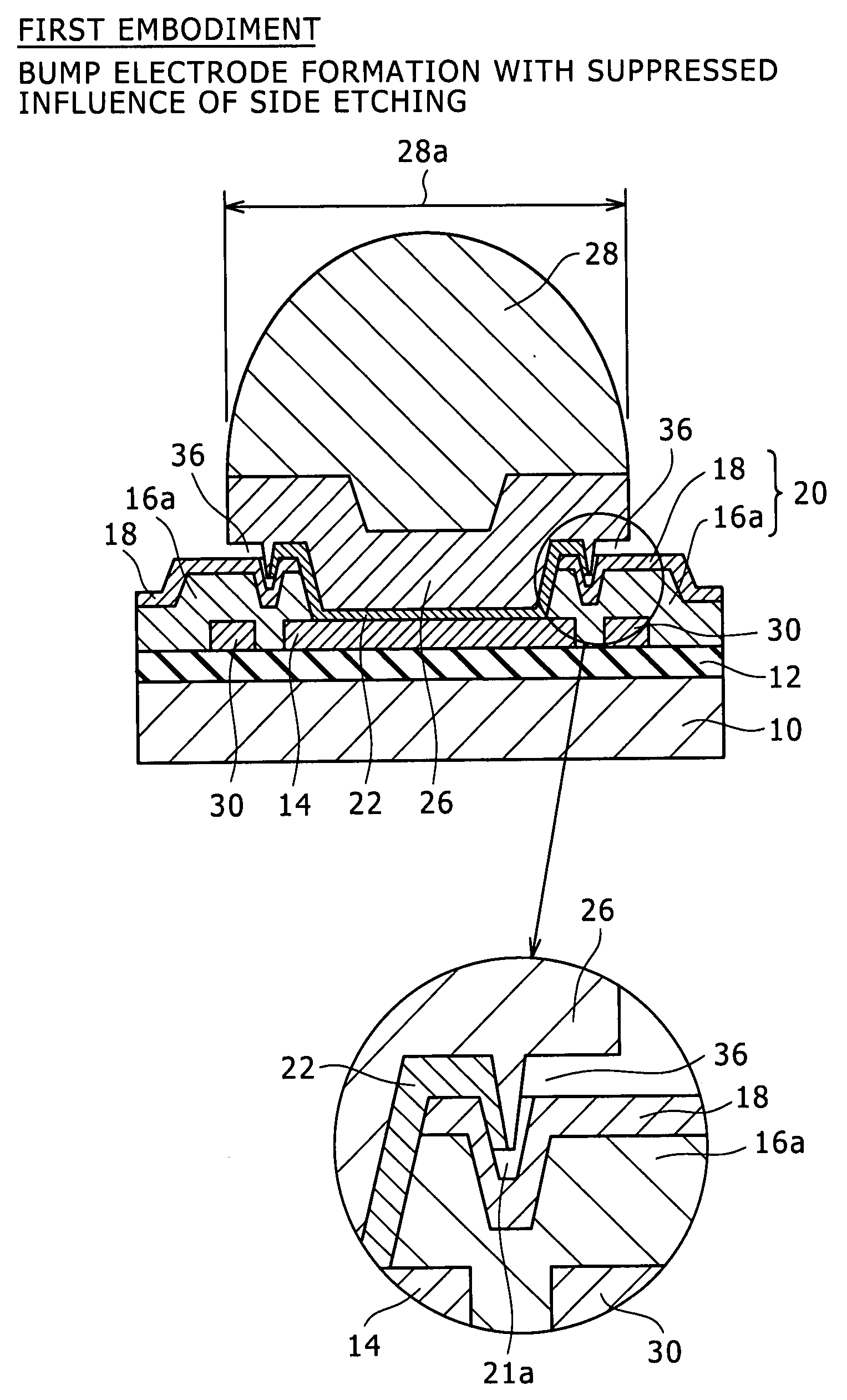
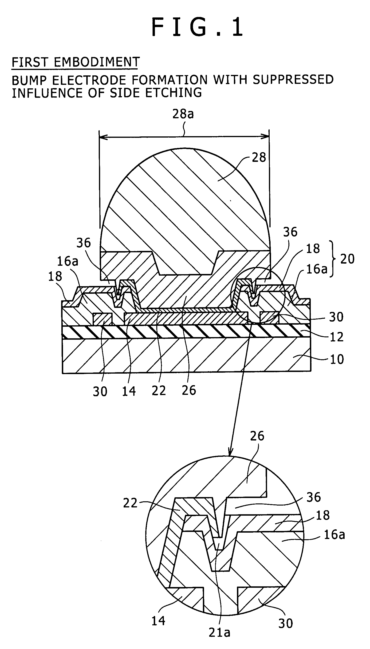
[0081]In a first embodiment of the present invention, a ring barrier 30 surrounding a pad electrode 14 is formed, and a bump electrode (protruding electrode) is formed above the pad electrode and the barrier. The barrier is to increase the length and area of the continuous part of an underlying metal layer and to suppress the influence of the occurrence of side etching, similarly to the respective subsequent embodiments. The form of the barrier formation differs among the following respective embodiments, and will be explained in detail in the descriptions of the embodiments.

[0082]In the present embodiment, the diameter of a pad electrode over which a bump electrode is to be formed is set smaller than that of the bump electrode. Furthermore, e.g. a metal pattern is disposed as a ring barrier in such a manner as to surround the pad electrode (in a ring manner for example). The ring barrier provided along the outline of the pad electrode is formed on the same plane as that on which th...

second embodiment

[0139]In a second embodiment of the present invention, projection and recess ring barriers are formed by using a passivation layer 20 on the inner periphery of a pad electrode 14, and a bump electrode 28 is formed above the pad electrode and the barriers. Specifically, these projection and recess ring barriers are formed on the pad electrode along the circumferential direction of an opening, and are formed at positions inside the projection of the bump electrode (projection to the plane on which the pad electrode is formed).

[0140]In the present embodiment, in a passivation layer on the pad electrode over which the bump electrode is to be formed, a center first opening (e.g., a circular opening, this opening is equivalent to the opening in the first embodiment) and a second opening (e.g., a circular ring opening) for forming a barrier surrounding the first opening are simultaneously formed (the diameter of the first opening and the outer diameter of the second opening are smaller tha...

third embodiment

[0165]In a third embodiment of the present invention, on a passivation layer 20 existing outside an opening 15a that exposes a part of a pad electrode 14 and on the periphery of the pad electrode 14, a ring projection barrier 34 is formed along the circumferential direction of the opening 15a. A bump electrode is formed above the pad electrode and the barrier 34. That is, the ring projection is formed at the outer periphery of the opening, and disposed on the passivation layer on the inner periphery of the pad electrode. The ring barrier 34, which is formed on the passivation layer 20 outside the opening 15a, is formed at a position inside the projection of the bump electrode (projection to the plane on which the pad electrode is formed) and between the bump electrode and the passivation layer.

[0166]In the present embodiment, an opening of which diameter is smaller than that of the bump electrode is formed in the passivation layer. On the passivation layer outside this opening, e.g....


PUM


Abstract

Herein disclosed an electronic component having a passivation layer in which an opening that exposes a part of a pad electrode is formed, an underlying metal layer formed on the pad electrode and the passivation layer, and a barrier metal layer formed on the underlying metal layer for an external connection electrode, the electronic component including a recess or/and a projection configured to be provided under the barrier metal layer outside or/and inside the opening, the underlying metal layer being formed on the recess or/and the projection and having a surface shape that follows the recess or/and the projection.

Description

CROSS REFERENCES TO RELATED APPLICATIONS[0001]The present invention contains subject matter related to Japanese Patent Application JP 2006-165722 filed with the Japan Patent Office on Jun. 15, 2006, the entire contents of which being incorporated herein by reference.BACKGROUND OF THE INVENTION[0002]1. Field of the Invention[0003]The present invention relates to electronic components and methods for mounting the same, and particularly to an electronic component having an external connection electrode that allows highly reliable electric connection because of prevention of the lowering of the bonding strength between the external connection electrode and a substrate, arising due to side etching (undercut) at the time of removal of the unnecessary part of an underlying metal layer by wet etching. The invention relates also to a semiconductor device employing this electronic component, and a method for manufacturing an electronic component.[0004]2. Description of the Related Art[0005]Th...

Claims


Application Information

Patent Timeline
IPC IPC(8): H01L23/48
CPCH01L24/03H01L24/05H01L24/11H01L24/12H01L2224/02255H01L2224/03019H01L2224/0401H01L2224/05018H01L2224/05082H01L2224/0555H01L2224/05552H01L2224/05557H01L2224/05558H01L2224/05624H01L2224/10126H01L2224/1147H01L2224/13007H01L2224/13099H01L2224/131H01L2224/13144H01L2224/16H01L2924/01004H01L2924/01005H01L2924/01011H01L2924/01013H01L2924/01014H01L2924/01015H01L2924/01022H01L2924/01028H01L2924/01029H01L2924/0103H01L2924/01032H01L2924/01033H01L2924/01046H01L2924/01047H01L2924/0105H01L2924/01051H01L2924/01074H01L2924/01078H01L2924/01079H01L2924/01082H01L2924/014H01L2924/05042H01L2924/19041H01L2924/19042H01L2924/19043H01L2924/01006H01L2924/01019H01L2924/01024H01L2224/05027H01L2224/05559H01L2224/05572H01L23/3192H01L2224/11902H01L2924/10253H01L2924/00014H01L2924/00012H01L2924/00H01L2224/02126H01L2224/05556H01L2224/13023H01L2224/02233H01L2224/05076H01L2224/05186
Inventor HARADA, YOSHIMICHIAOYAGI, AKIYOSHIASAMI, HIROSHI
Owner SONY CORP
Why Eureka
Try Eureka