Stacked semiconductor device

a semiconductor device and stacked technology, applied in semiconductor devices, digital storage, instruments, etc., can solve the problems of waveform distortion, high speed transmission, distorted dqs signal waveform, etc., to increase data transmission speed, reduce load on transmission lines, and increase data transmission speed

Inactive Publication Date: 2007-12-20
LONGITUDE SEMICON S A R L
View PDF3 Cites 49 Cited by
  • Summary
  • Abstract
  • Description
  • Claims
  • Application Information

AI Technical Summary

Benefits of technology

[0016] It is an object of the present invention to eliminate waveform distortion at high speed transmission in case of stacking a plural number of memory chips. That is, a first object of the present invention is relevant to the package substrate having the wiring for transmitting a data strobe signal.
[0017] It is another object of the present invention to eliminate signal skew of the data strobe signal transmitted between the memory chips upon data readout to secure a timing margin of the setup time and the hold time of the memory controller. That is, a second object of the present invention is relevant to the memory chip outputting a data strobe signal upon data readout.
[0021] According to the present invention, it is possible to increase the data transmitting speed in a stacked semiconductor device including plural memory chips stacked together.
[0022] According to the first aspect of the present invention, data strobe signals are not branched, so that the load on the transmission line is decreased, thereby allowing the recording capacity and the data transmitting speed to be increased.
[0023] According to the second aspect of the present invention, the frequency of the clock signal may be increased regardless of the signal skew between the clock signal and the data strobe signal, thereby increasing the recording capacity and the data transmitting speed.

Problems solved by technology

However, the routine stacked semiconductor devices are plagued with the following problem.
Thus, with the routine stacked semiconductor devices, the waveform of the DQS signal is distorted and deteriorated because of reflection at the branch point to render high speed transmission difficult.
In this case, the problem of waveform distortion is presented at high speed transmission because of reflection caused by a branched path 106.

Method used


Image

  • Stacked semiconductor device
  • Stacked semiconductor device
  • Stacked semiconductor device

Examples


first example

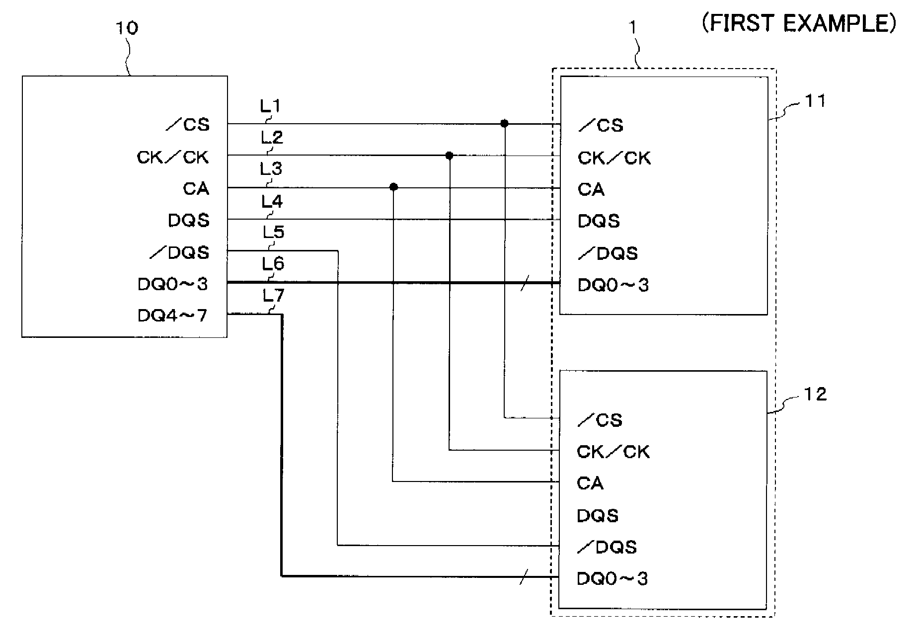
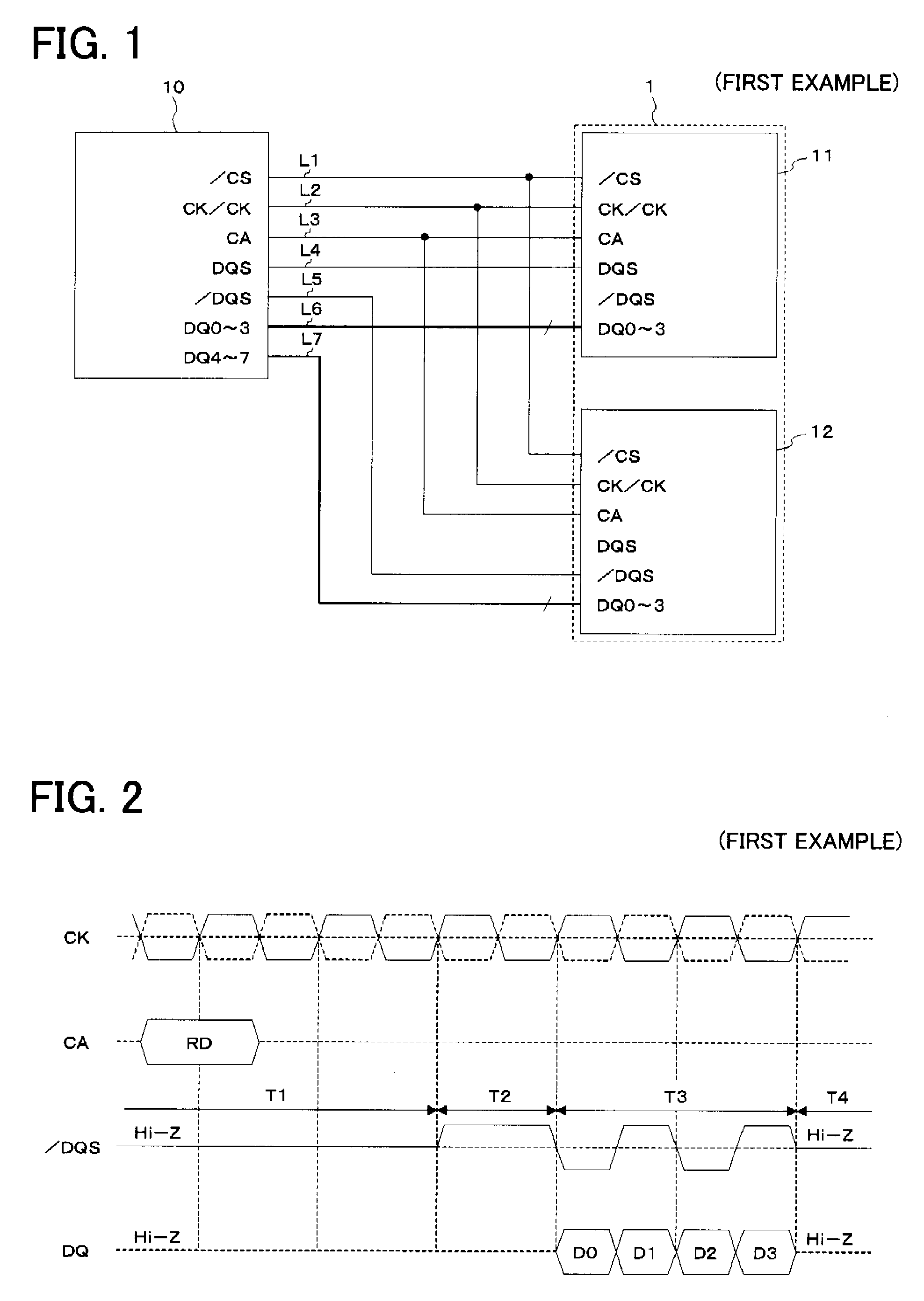
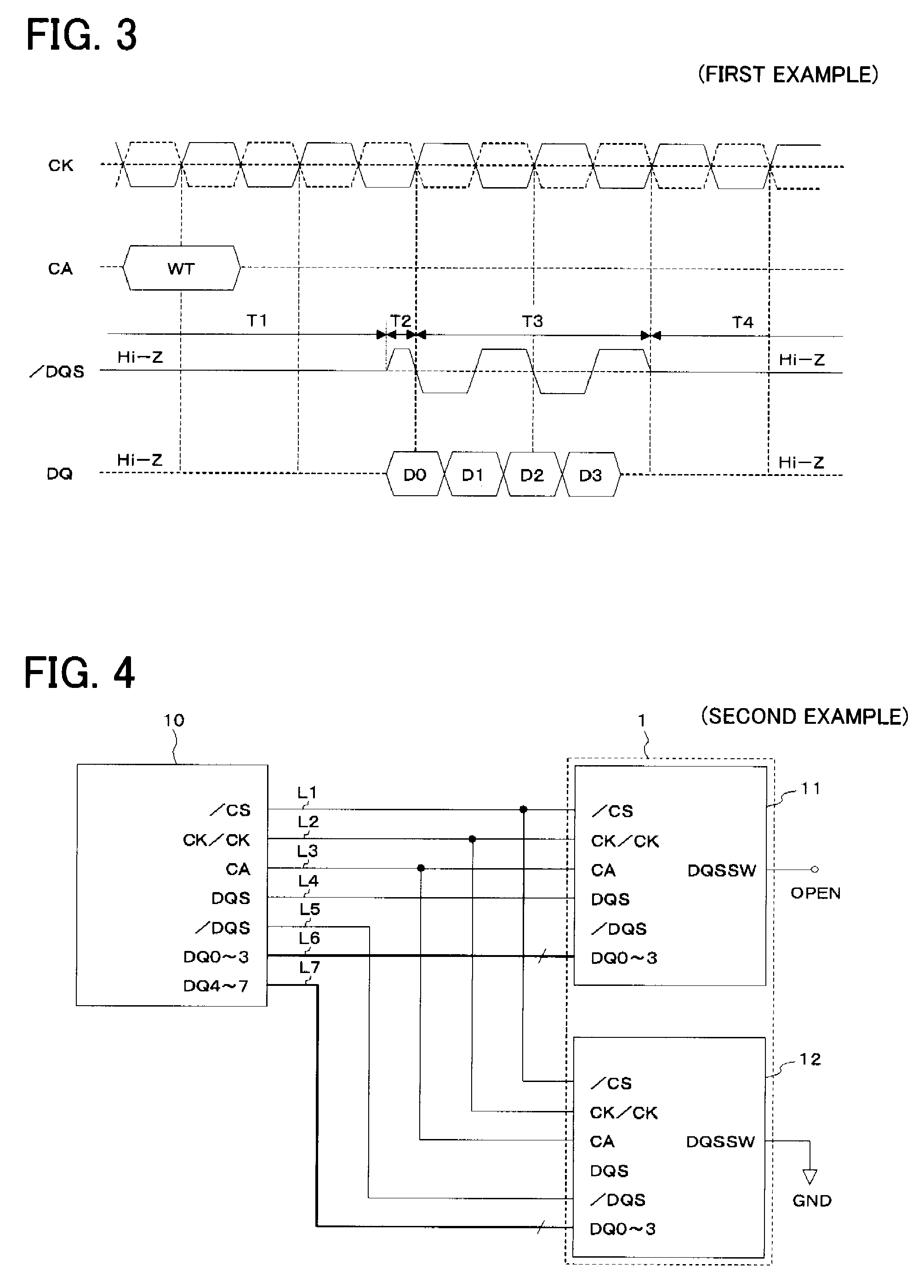
[0052] A stacked semiconductor device of a first example of the present invention is now described with reference to the drawings. FIG. 1 depicts a block diagram schematically showing the constitution of the stacked semiconductor device according to the first example of the present invention.

[0053] Referring to FIG. 1, a stacked semiconductor device 1 is a DDR2 SDRAM of a ×8 bit constitution comprising two DDR2 SDRAM chips stacked together. These two DDR2 SDRAM chips are memory chips 11, 12 each being of a ×4 bit constitution. The stacked semiconductor device 1 is designed to control the input / output of data signals (DQ signals) of the memory chips 11, 12, based on data strobe signals (DQS signals) and inverted data strobe signals ( / DQS signals) from a memory controller 10. In the stacked semiconductor device 1, a set of one DQS signal and one / DQS signal is allocated to each 8-bit data. The stacked semiconductor device 1 is electrically connected to the memory controller 10 via a ...

second example

[0062] A stacked semiconductor device of a second example of the present invention is now described with reference to the drawings. FIG. 4 depicts a block diagram schematically showing the constitution of the stacked semiconductor device according to the second example of the present invention.

[0063] In the second example of the stacked semiconductor device 1, as in the first example, described above, two DDR2 SDRAM chips, as memory chips 11, 12, each being of a ×4 bit constitution, are stacked together to constitute a DDR2 SDRAM of a ×8 bit constitution. The stacked semiconductor device 1 is configured for controlling inputting / outputting of the data signals (DQ signals) of the memory chips 11, 12, based on the data strobe signal (DQS signal) and the inverted data strobe signal ( / DQS signal) from the memory controller 10. The present second example of the stacked semiconductor device I differs from the above-described first example in that, in the memory chips 11, 12, the DQS sign...

third example

[0066] A stacked semiconductor device of a third example of the present invention is now described with reference to the drawings. FIG. 5 depicts a block diagram schematically showing the constitution of the stacked semiconductor device according to the third example of the present invention. FIG. 6 is a block diagram showing a circuit connected to a DQS signal pad of a second memory chip in the stacked semiconductor device of the third example of the present invention.

[0067] In the present third example of the stacked semiconductor device, as in the first example, two DDR2 SDRAM chips, each of the ×4 bit constitution, providing the memory chips 11, 12, are stacked together to provide a DDR2 SDRAM chip of the ×8 bit constitution. The stacked semiconductor device 1 is designed to control the inputting / outputting of the data signals (DQ signals) of the memory chips 11, 12, based on the data strobe signal (DQS) signal and the inverted data strobe signal ( / DQS signal) from the memory ...


PUM


Abstract

Stacked semiconductor device includes plural memory chips, stacked together, in which waveform distortion at high speed transmission is removed. Stacked semiconductor device 1 includes plural memory chips 11, 12 stacked together. Data strobe signal (DQS) and inverted data strobe signal ( / DQS), as control signals for inputting / outputting data twice per cycle, are used as two single-ended data strobe signals. Data strobe signal and inverted data strobe signal mate with each other. Data strobe signal line for the data strobe signal L4 is connected to data strobe signal (DQS) pad of first memory chip 11. Inverted data strobe signal line for / DQS signal L5 is connected to inverted data strobe signal ( / DQS) pad of second memory chip 12.

Description

REFERENCE TO RELATED APPLICATIONS [0001] The present application is claiming the priority of the earlier Japanese patent application No. 2006-163735 filed on Jun. 13, 2006, the entire disclosure thereof being incorporated herein by reference thereto. FIELD OF THE INVENTION [0002] This invention relates to a stacked semiconductor device including a plural number of memory chips stacked together in lamination. More particularly, this invention relates to a stacked semiconductor device including memory chips of, for example, a DDR SDRAM or a DDR2 SDRAM. BACKGROUND OF THE INVENTION [0003] In a stacked semiconductor device including a plural number of memory chips stacked together, such as a memory module, an SDRAM (Synchronous Dynamic Random Access Memory), latching a variety of control signals by a rising edge of a fundamental input clock signal (CK signal) to input / output data in synchronization with the CK signal, is in widespread use. The SDRAM uses only the rising edge of the CK si...

Claims


Application Information

Patent Timeline
Patent Type & Authority Applications(United States)
IPC IPC(8): G11C5/06G11C7/00G11C8/00
CPCG11C5/02G11C5/04G11C7/02H01L25/105H01L2924/15311H01L2924/0002H01L2924/15331H01L2924/00
Inventor NISHIO, YOJIUEMATSU, YUTAKAFUNABA, SEIJIOSAKA, HIDEKIHARA, TSUTOMUAOKI, KOICHIRO
Owner LONGITUDE SEMICON S A R L
Why Eureka
Try Eureka