

Method for manufacturing semiconductor device
- Summary
- Abstract
- Description
- Claims
- Application Information
AI Technical Summary
Benefits of technology
Problems solved by technology
Method used
Image

Examples
embodiment modes
[0065] Hereinafter, Embodiment Modes of the present invention will be described with reference to the drawings. Note that the present invention can be carried out in many different modes. It is easily understood by those skilled in the art that modes and details disclosed herein can be modified in various ways without departing from the spirit and the scope of the present invention. Therefore, it should be noted that the present invention should not be interpreted as being limited to the description of the embodiment modes given below. Note that like portions or portions having a like function are denoted by the same reference numerals through drawings, and therefore, description thereon is omitted.
embodiment mode 1
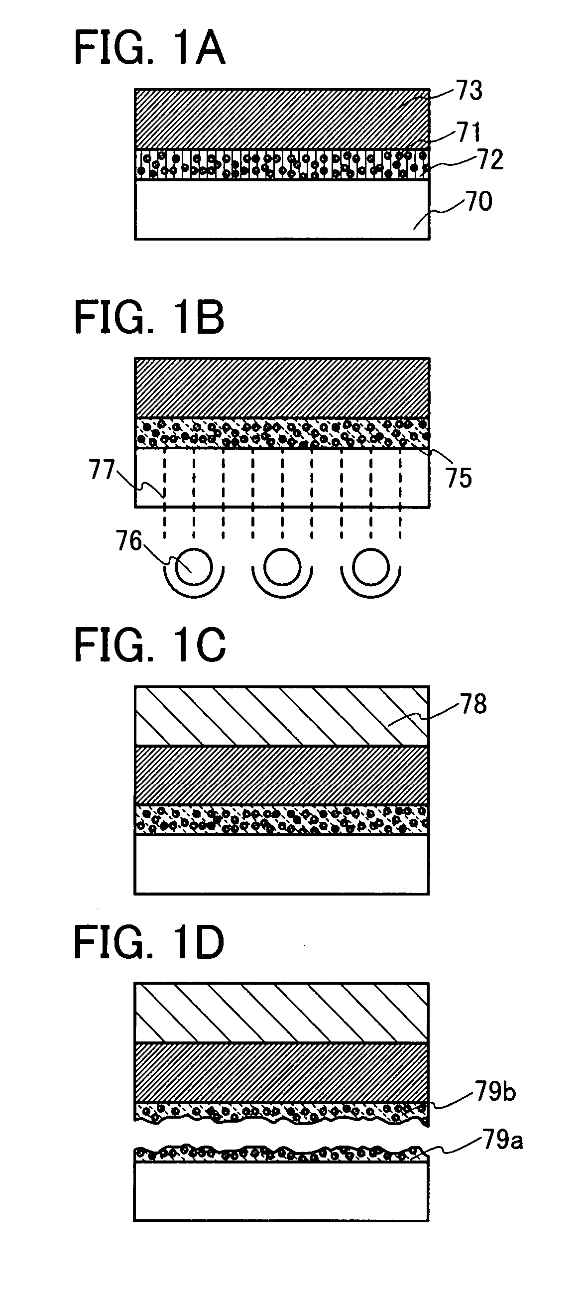
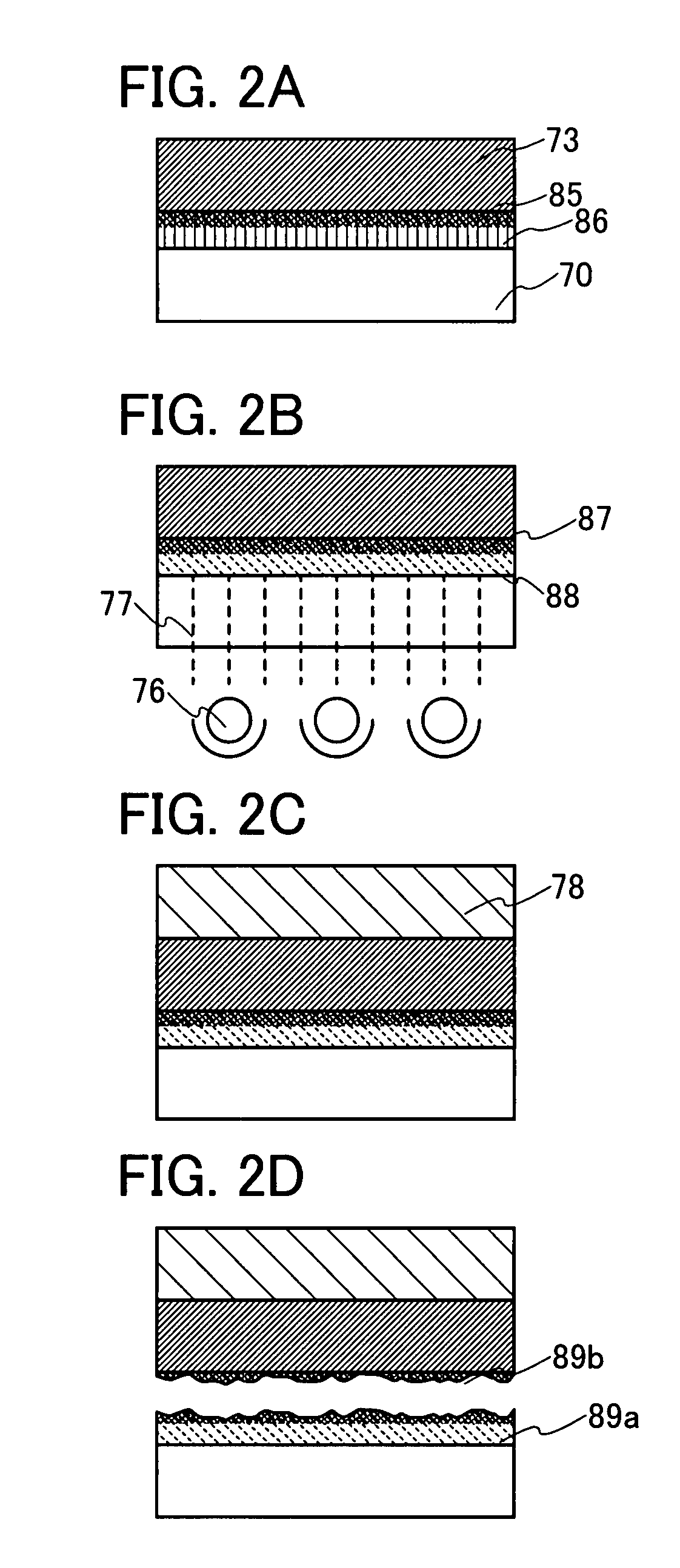
[0066] An embodiment mode of the present invention is described with reference to FIGS. 1A to 1D.
[0067] According to the present invention, when an element layer is formed over a substrate, an organic compound layer including a substance having a photocatalyst function (hereinafter, also a photocatalyst substance) is provided between the substrate and the element layer. The photocatalyst substance absorbs light, and thus, the photocatalyst substance is activated by the light. The activation energy acts on peripheral organic compound, and as a result, changes and modifies properties of the organic compound. In other words, by the energy of the activated photocatalyst substance (oxidizability), a carbon-hydrogen bond and a carbon-carbon bond of such organic compound are separated, and a part of the organic compound becomes carbon dioxide and water, and is degassed. Consequently, the organic compound layer including a photocatalyst substance becomes rough and is separated (sectioned) ...
embodiment mode 2
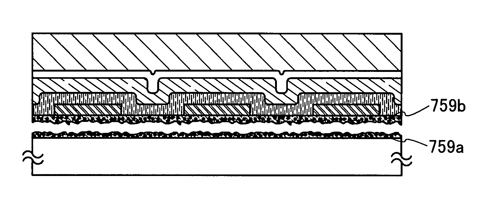
[0101] Embodiment Mode 2 will explain one structural example of a display device to which a transfer process of the present invention is applied, with reference to drawings. More specifically, a case where a structure of a display device is a passive matrix type will be shown.
[0102] The display device includes first electrode layers 751a, 751b, and 751c extending in a first direction; an electroluminescent layer 752 provided to cover the first electrode layers 751a, 751b, and 751c; and second electrode layers 753a, 753b, and 753c extending in a second direction perpendicular to the first direction (FIG. 5A). The electroluminescent layer 752 is provided between the first electrode layers 751a, 751b, and 751c and the second electrode layers 753a, 753b, and 753c. In addition, an insulating layer 754 functioning as a protection film is provided so as to cover the second electrode layers 753a, 753b, and 753c. The element layer including the first electrode layers 751a, 751b and 751c, th...
PUM
 Abstract
Description
Claims
Application Information