Pick-up structure for dram capacitors and dram process

a technology of dram cells and pick-up structures, applied in the field of dram process, can solve problems such as limiting the integration degree, and achieve the effect of simplifying the dram process and increasing the integration degree of the dram

Active Publication Date: 2007-12-27
UNITED MICROELECTRONICS CORP
View PDF4 Cites 24 Cited by
  • Summary
  • Abstract
  • Description
  • Claims
  • Application Information

AI Technical Summary

Benefits of technology

[0008]This invention also provides a capacitor pick-up structure for a DRAM array, which includes a dummy capacitor at an edge or a corner of the memory array area as a connector to the doped band so that the integration degree of DRAM is increased.

Problems solved by technology

However, the prior-art method limits the integration degree because the deep N-well requires a certain lateral area even when the memory cell dimension is reduced, and is quite tedious due to the multiple ion implantations.

Method used


Image

  • Pick-up structure for dram capacitors and dram process
  • Pick-up structure for dram capacitors and dram process
  • Pick-up structure for dram capacitors and dram process

Examples


Embodiment Construction

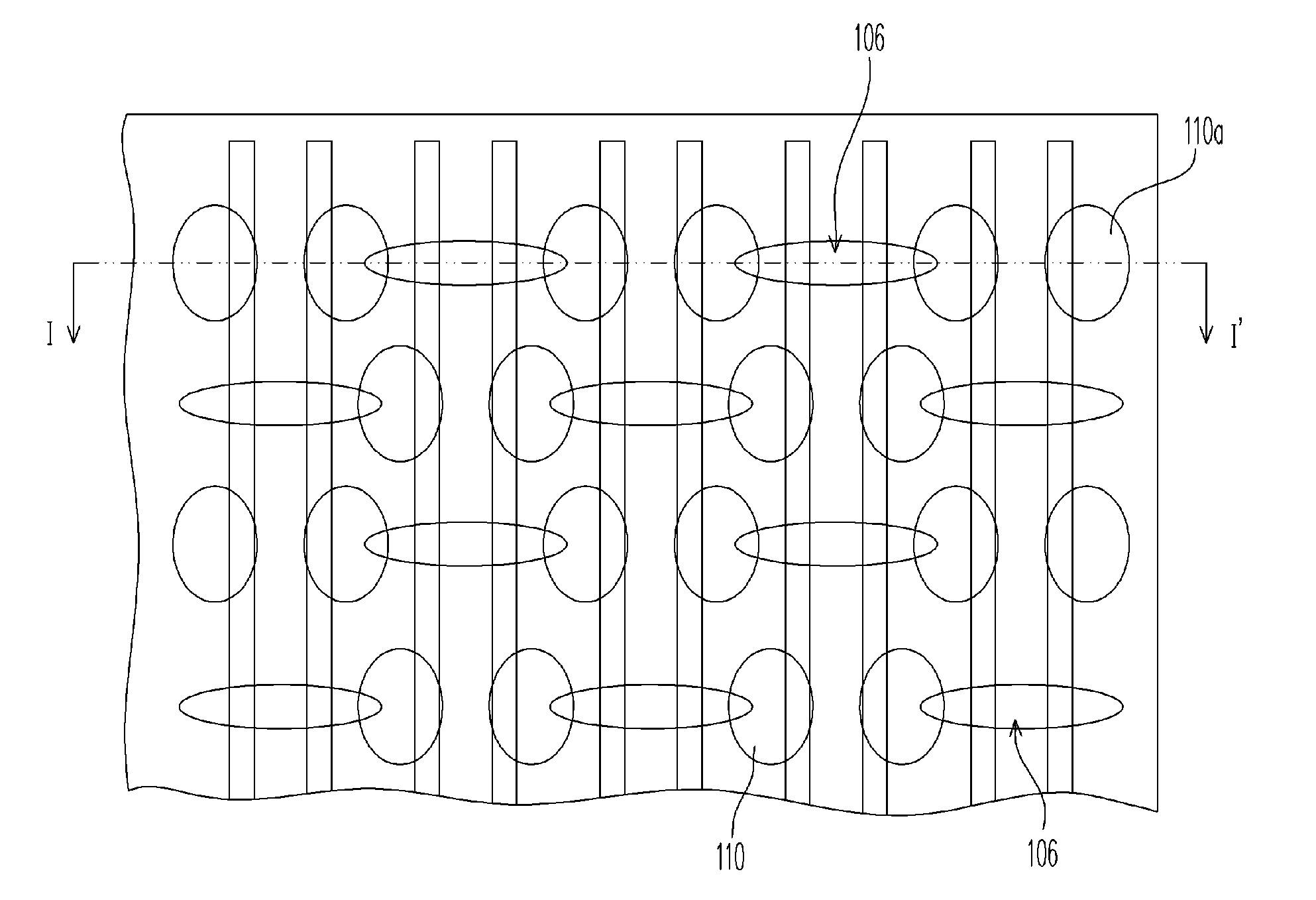
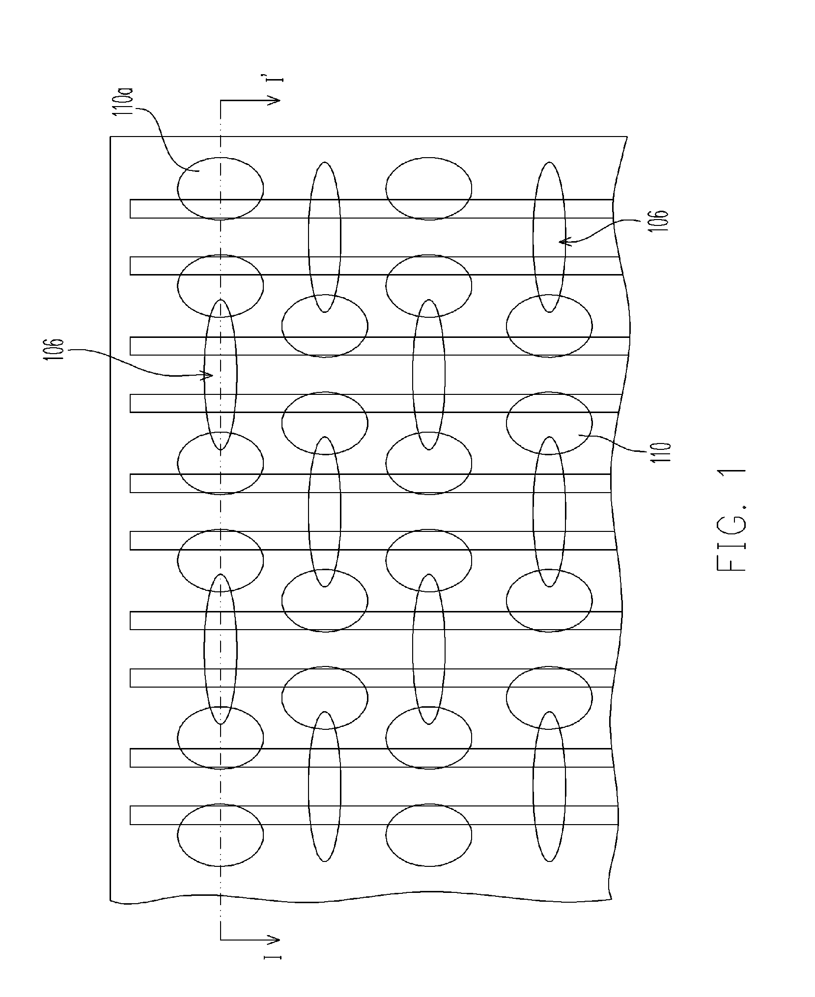
[0032]FIG. 1 illustrates a top view of a DRAM layout according to an embodiment of this invention. FIGS. 2A-2E illustrate a DRAM process according to a preferred embodiment of this invention.

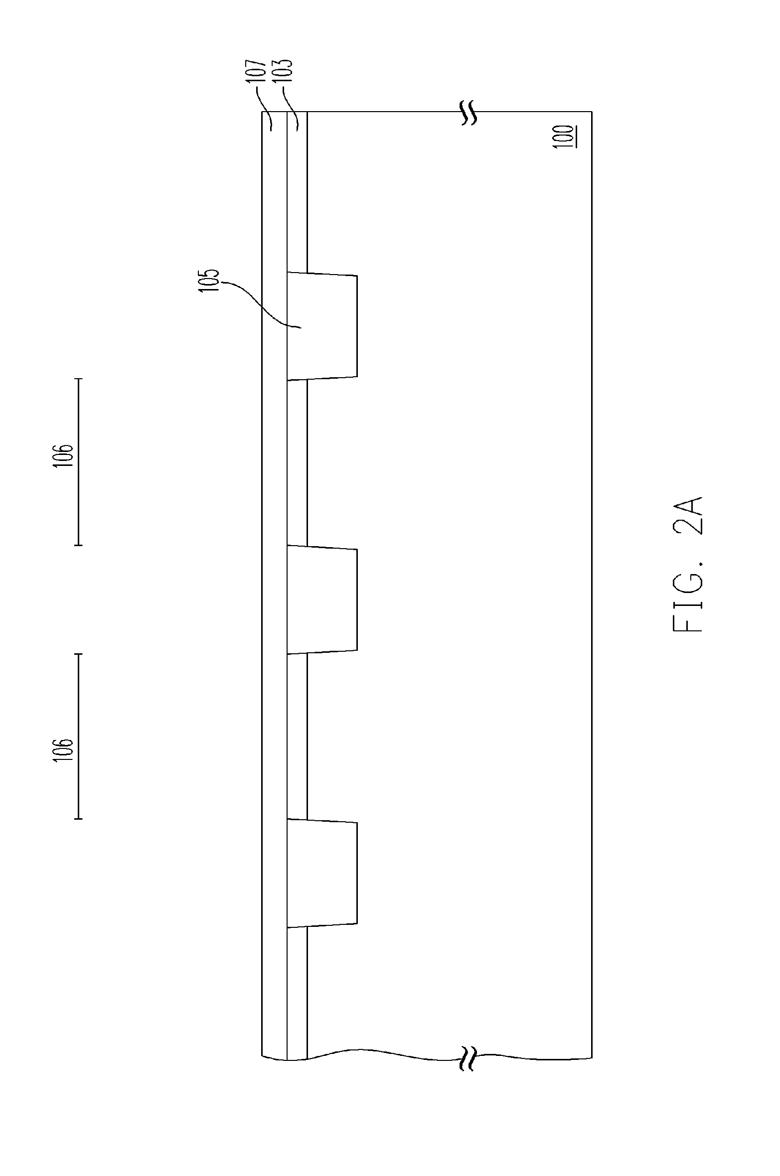
[0033]Referring to FIGS. 1 and 2A, a substrate 100 like a silicon substrate is provided, and then a hard mask layer 103 is formed on the substrate 100. The hard mask layer 130 may include silicon nitride (SiN) and may be formed through CVD. An isolation structure 105 defining active areas 106 is then formed in the hard mask layer 103 and the substrate 100, possibly being a shallow trench isolation (STI) structure and possibly including silicon oxide. Before the hard mask layer 103 is formed, a pad layer (not shown) may be formed on the substrate 100. The process for forming the pad layer to the isolation structure 105 can be any suitable process having been applied the prior art.

[0034]Optionally, another hard mask layer 107 is further formed on the substrate 100 if required, possibly including S...


PUM


Abstract

A pick-up structure for DRAM capacitors and a DRAM process are described. A substrate with trenches therein is provided, wherein the trenches include a first trench and the sidewall of each of the trenches is formed with a dielectric layer thereon. A conductive layer is formed on the surfaces of the substrate and the trenches, and then a patterned photoresist layer is formed on the conductive layer filling in the trenches and further covering the first trench. The exposed conductive layer is removed to form bottom electrodes in the trenches, and then the patterned photoresist layer is removed. A capacitor dielectric layer is formed on each bottom electrode, and then top electrodes are formed on the substrate filling up the trenches. A contact is then formed on the bottom electrode in the first trench, electrically connecting the substrate via the bottom electrode.

Description

BACKGROUND OF THE INVENTION[0001]1. Field of Invention[0002]The present invention relates to a semiconductor structure and its fabrication. More particularly, this invention relates to a pick-up structure for capacitors of DRAM cells and to a DRAM process including the formation of the capacitor pick-up structure.[0003]2. Description of Related Art[0004]There are generally two types of capacitors for DRAM cells, including stacked capacitor and deep-trench (DT) capacitor, wherein the DT capacitor is formed in the substrate and the capacitance thereof can be easily increased by increasing the trench depth, so that much less lateral area is required.[0005]Since the trenches of the trench capacitors are formed quite deep, an N-band is formed quite deep in the substrate to electrically connect the bottom electrodes of all capacitors. To pick up such a deep N-band, in the prior art, multiple ion implantations of different doses and energies are conducted to form a wide deep N-well, and th...

Claims


Application Information

Patent Timeline
Patent Type & Authority Applications(United States)
IPC IPC(8): H01L29/94
CPCH01L21/743H01L29/66181H01L27/10894H01L27/1087
Inventor SU, YI-NANYANG, CHIN-SHENG
Owner UNITED MICROELECTRONICS CORP
Why Eureka
Try Eureka