
Apparatus for reducing offset voltage drifts in a charge amplifier circuit

a charge amplifier and offset voltage technology, applied in the field of sensing circuits, can solve the problems of significant offset drift at output vb>0/b>, unacceptably high for most, if not all, precision applications, etc., and achieve the effect of reducing offset voltage drift and lowering any offset voltage dri

Inactive Publication Date: 2007-12-27
BAE SYST INFORMATION & ELECTRONICS SYST INTERGRATION INC
View PDF2 Cites 11 Cited by
  • Summary
  • Abstract
  • Description
  • Claims
  • Application Information

AI Technical Summary

Benefits of technology

[0008]In accordance with a preferred embodiment of the present invention, an apparatus for reducing offset voltage drifts in a charge amplifier circuit includes a charge amplifier circuit and a bias current compensation circuit. The bias current compensation circuit supplies bias current to lower any offset voltage drift at the output of the charge amplifier.

Problems solved by technology

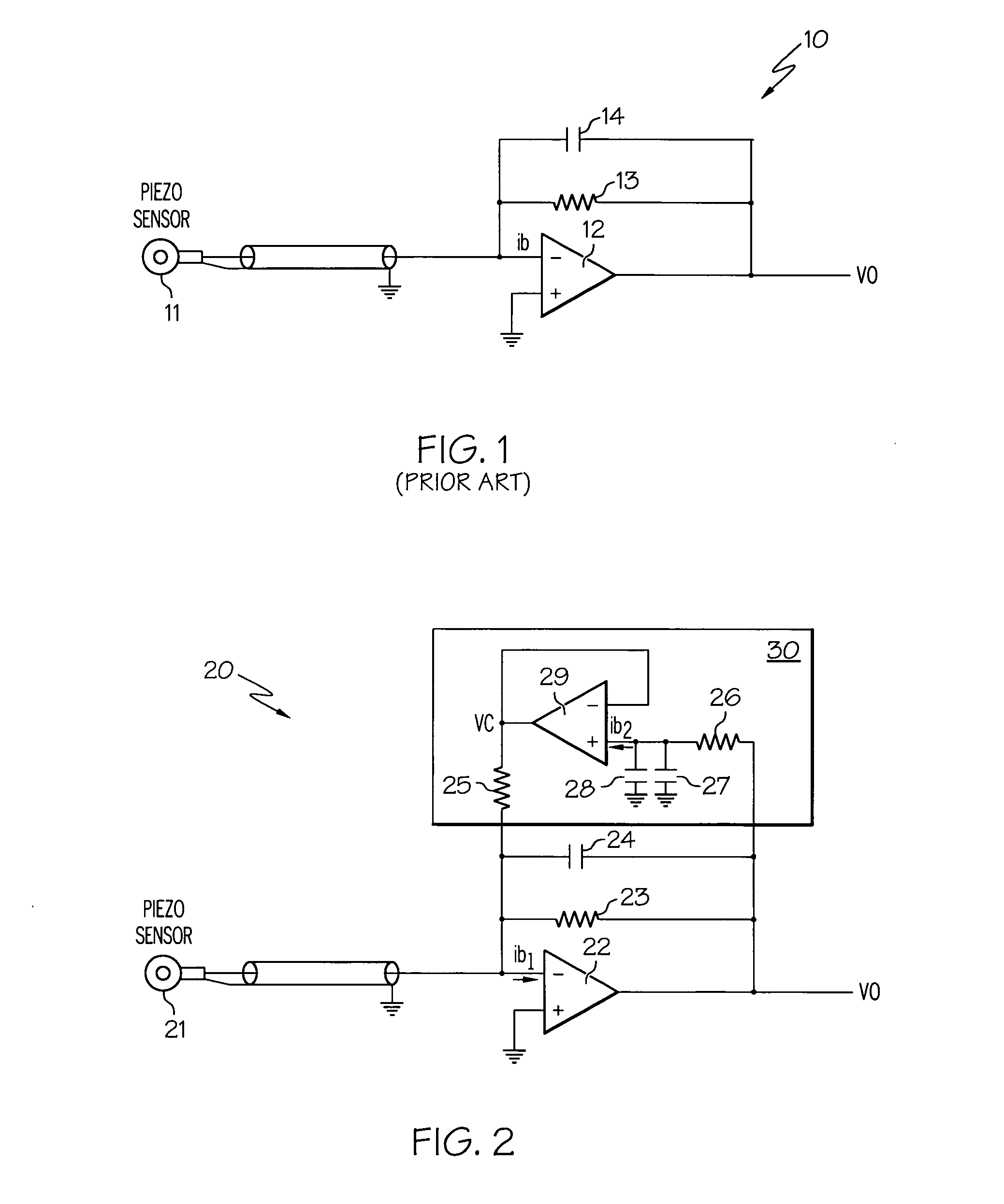
Because capacitor 14 requires a relatively small capacitance C1 to achieve a reasonable output voltage, one problem with charge amplifier circuit 10 is that the resistance R1 of resistor 13 must be very large in order to achieve a reasonable low-frequency cutoff.
In addition, the change in the input bias / offset current ib over temperature can also result in a significant offset drift at output V0.
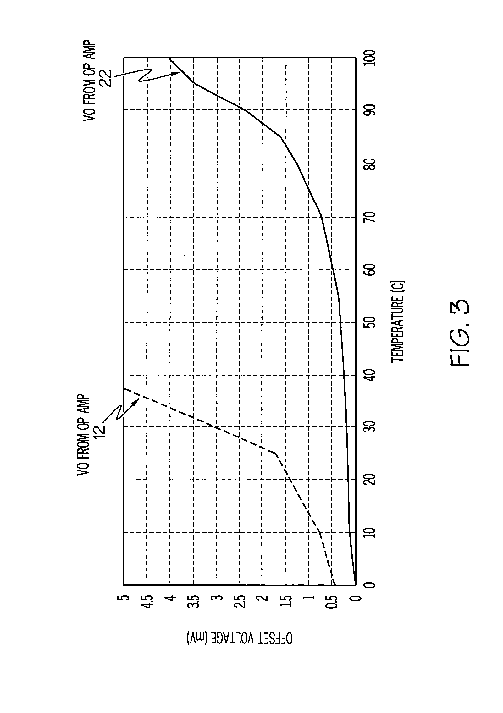
Even when using a JFET operational amplifier having an input bias / offset current and drift (per degree Celsius) in the pico range, the DC offset and offset drift (per degree Celsius) at output V0 can end up being in the milli range, which is unacceptably high for most, if not all, precision applications.

Method used


Image

  • Apparatus for reducing offset voltage drifts in a charge amplifier circuit
  • Apparatus for reducing offset voltage drifts in a charge amplifier circuit
  • Apparatus for reducing offset voltage drifts in a charge amplifier circuit

Examples


Embodiment Construction

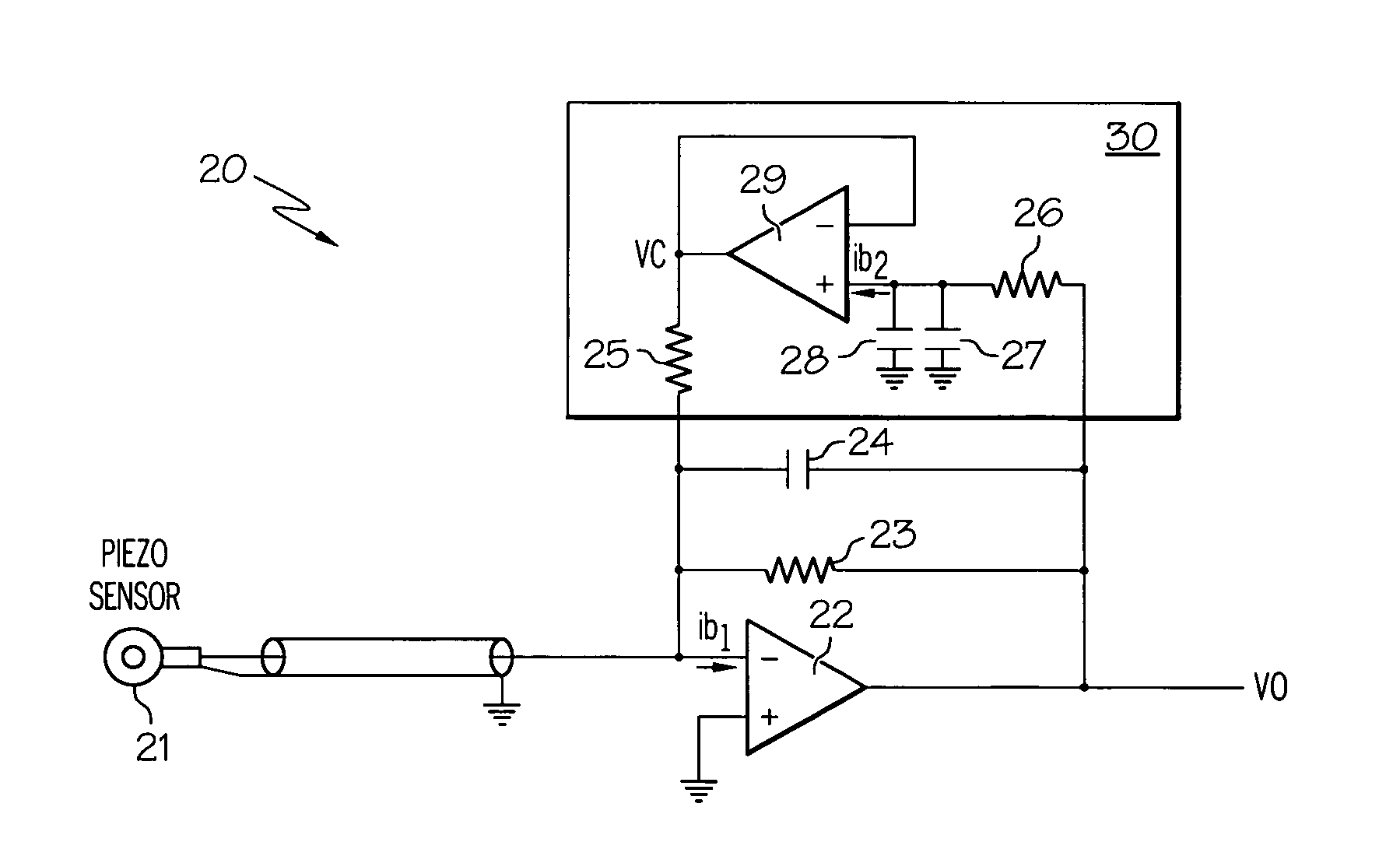
[0014]With reference now to FIG. 2, there is illustrated a schematic diagram of a charge amplifier circuit, in accordance with a preferred embodiment of the present invention. As shown, a charge amplifier circuit 20 includes a piezoelectric sensor 21, an operational amplifier 22, a resistor 23 and a capacitor 24. Charge amplifier circuit 20 also includes a bias current compensation circuit 30 having an operational amplifier 29, resistors 25-26, and capacitors 27-28. Within bias current compensation circuit 30, a node VC tracks the voltage changes at output V0 (due to DC offset and offset drift) that are significantly below the cutoff frequency of a low-pass filter formed by resistor 25 and capacitors 27-28.

[0015]Any voltage change at node VC, through negative feedback, counteracts and limits the (low-frequency) voltage change at output V0. Thus, any DC offset caused by input bias / offset current will be attenuated by the loop gain 1+R1 / R2, where R1 is the resistance of resistor 23 an...


PUM


Abstract

An apparatus for reducing offset voltage drifts in a charge amplifier circuit is disclosed. The apparatus includes a charge amplifier circuit and a bias current compensation circuit. The bias current compensation circuit supplies bias current to lower any offset voltage drift at the output of the charge amplifier.

Description

STATEMENT OF GOVERNMENT INTEREST[0001]The present invention was made with United States Government support under contract number 03-009019-47236. The United States Government has certain rights in the present invention.BACKGROUND OF THE INVENTION[0002]1. Technical Field[0003]The present invention relates to sensing circuits in general, and in particular to charge amplifier circuits. Still more particularly, the present invention relates to an apparatus for reducing offset voltage drifts in a charge amplifier circuit.[0004]2. Description of Related Art[0005]Referring now to the drawings and in particular to FIG. 1, there is illustrated a schematic diagram of a charge amplifier circuit capable of converting the output of a piezoelectric charge mode sensor to a corresponding voltage, according to the prior art. As shown, a charge amplifier circuit 10 includes a piezoelectric sensor 11 that is capable of producing a charge proportional to an applied mechanical force. As the voltage at o...

Claims


Application Information

Patent Timeline
Patent Type & Authority Applications(United States)
IPC IPC(8): H03F3/45
CPCH03F3/45475H03F3/45973H03F3/70H03F2203/45526H03F2203/45138H03F2203/45212H03F2203/45521H03F2200/261
Inventor BLUMEN, ARTHUR RUSSELLKNOWLES, KENNETH R.
Owner BAE SYST INFORMATION & ELECTRONICS SYST INTERGRATION INC
Learn More