

Digital adjustment of an oscillator
- Summary
- Abstract
- Description
- Claims
- Application Information
AI Technical Summary
Benefits of technology
Problems solved by technology
Method used
Image

Examples
Embodiment Construction
)
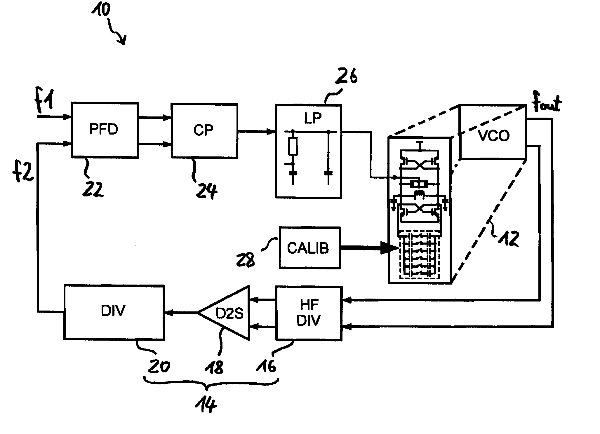
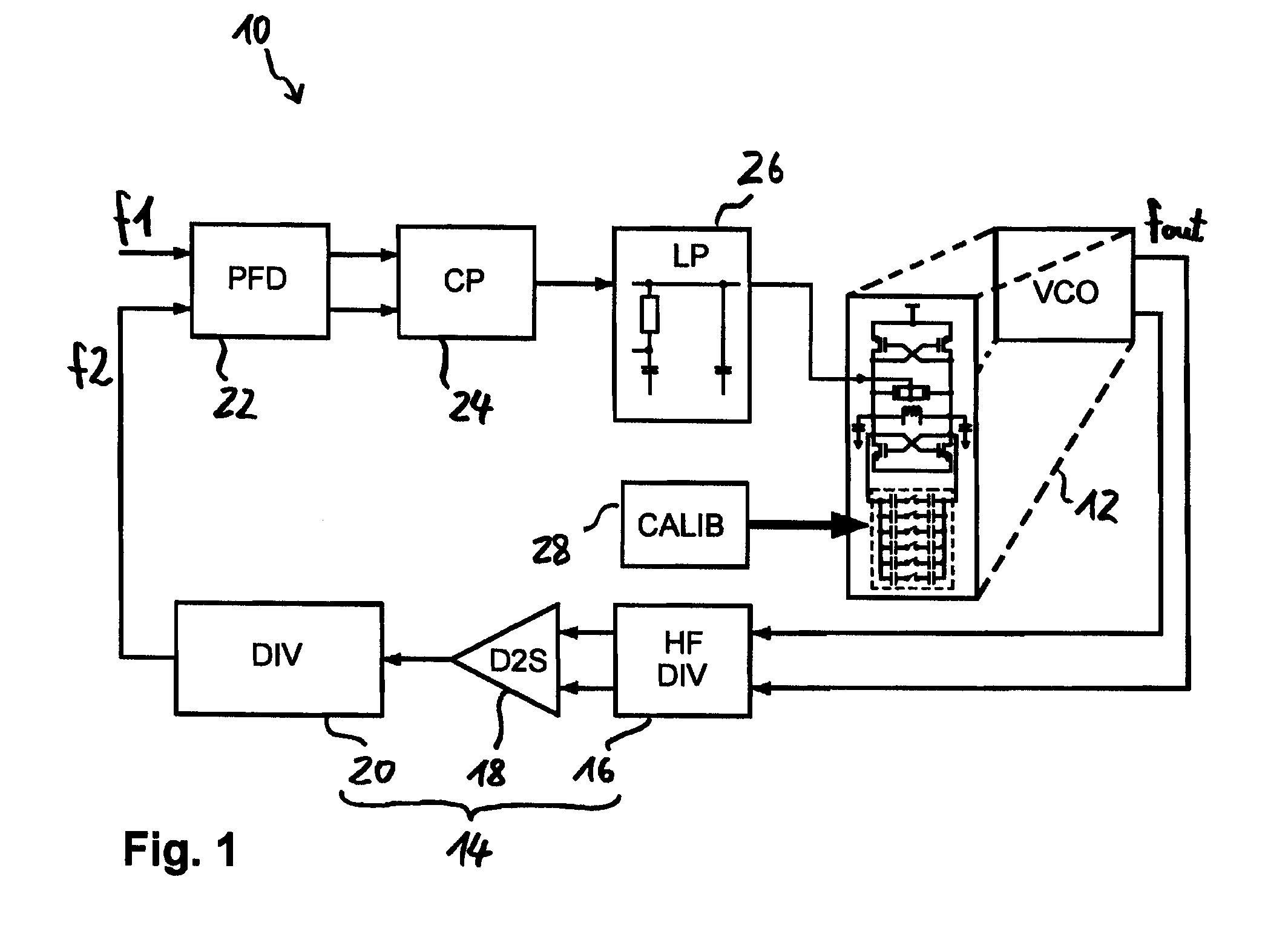
[0032]FIG. 1 shows a phase lock loop 10, in what follows designated as PLL 10, with a structure known per se. Such a PLL represents a preferred application environment for the circuit arrangement according to the invention described further below for the adjustment of an oscillation frequency.
[0033] The PLL 10 comprises a voltage controlled oscillator (VCO) 12 for the generation of a PLL output signal with a frequency fout, which is used for parts of a circuit, not represented in FIG. 1, of a “mixed signal” circuit arrangement, which also contains the components represented in FIG. 1.
[0034] The output signal of the VCO 12 is fed via a feedback path 14 consisting of a first frequency divider 16, a converter element 18 and a second divider 20 to an input of a phase detector or phase comparator 22 as a feedback signal with a frequency f2. An input clock signal (PLL input signal) is applied to another input of the phase detector 22; this signal has a frequency f1.
[0035] The fed-back...
PUM
 Abstract
Description
Claims
Application Information