Substrate processing method and substrate processing apparatus

a substrate processing and processing method technology, applied in the direction of electrical apparatus, basic electric elements, semiconductor/solid-state device manufacturing, etc., can solve the problem of etching of the substrate of silicon substra

Active Publication Date: 2008-01-03
TOKYO ELECTRON LTD
View PDF5 Cites 97 Cited by
  • Summary
  • Abstract
  • Description
  • Claims
  • Application Information

AI Technical Summary

Benefits of technology

[0021]With the substrate processing apparatus according to the second aspect of the present invention, effects

Problems solved by technology

As a result, even the silicon

Method used


Image

  • Substrate processing method and substrate processing apparatus
  • Substrate processing method and substrate processing apparatus
  • Substrate processing method and substrate processing apparatus

Examples


first embodiment

[0028]First, an explanation will be given of a substrate processing system for carrying out a substrate processing method according to the present invention.

[0029]FIG. 1 is a plan view schematically showing the construction of the substrate processing system of this embodiment.

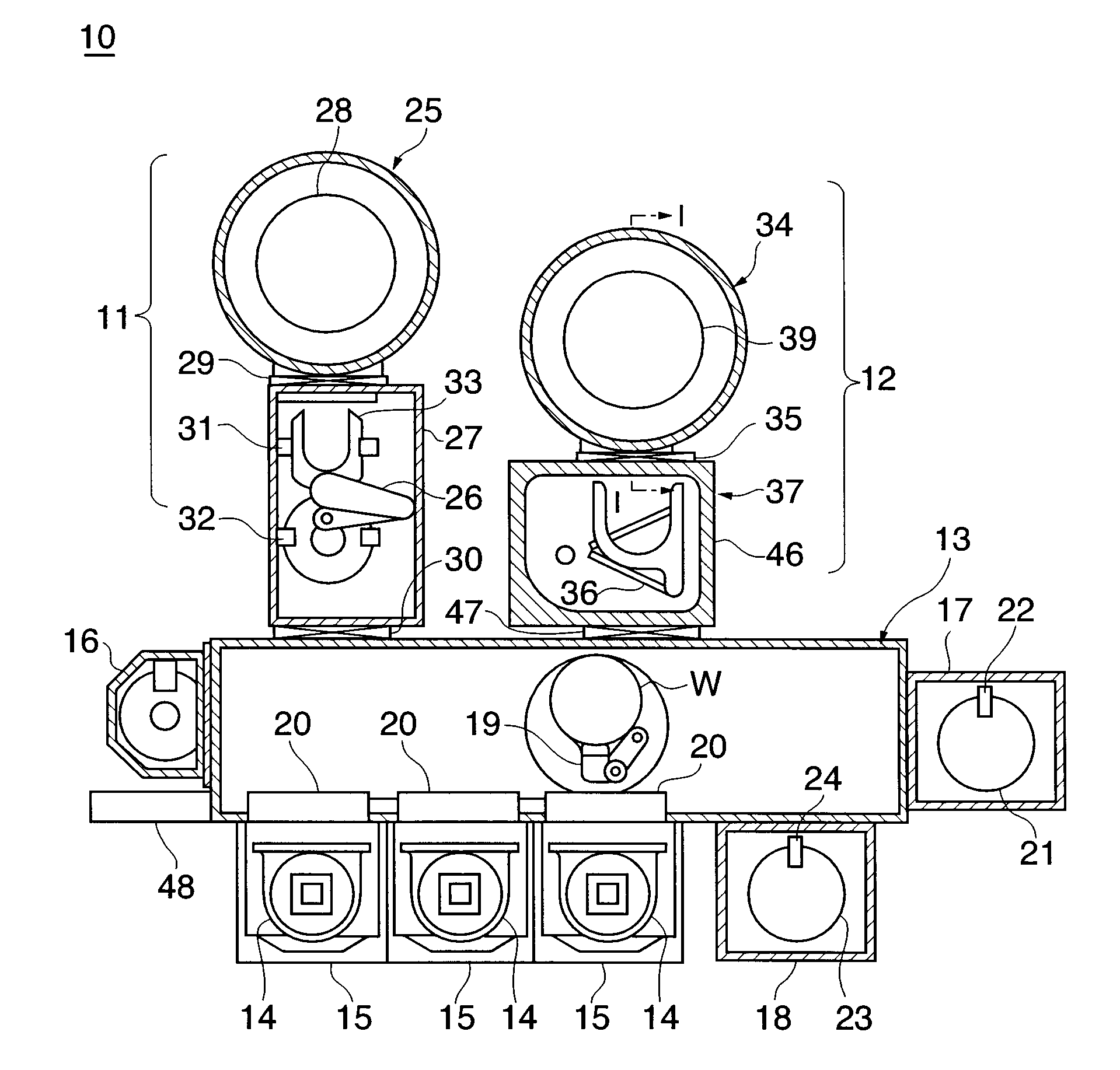
[0030]As shown in FIG. 1, the substrate processing system (substrate processing apparatus) 10 has a first process ship 11 for carrying out plasma processing on semiconductor device wafers W (substrates), hereinafter referred to simply as “wafers”, a second process ship 12 that is disposed parallel to the first process ship 11 and is for carrying out selective etching, described below, on the wafers W on which the plasma processing has been effected in the first process ship 11, and a loader unit 13 which is a rectangular common transfer chamber and to which the first and second process ships 11, 12 are connected.

[0031]In addition to the first and second process ships 11 and 12, there are connected to the loade...

second embodiment

[0072]Next, an explanation will be give of a substrate processing method according to this invention.

[0073]This embodiment is the same or similar in construction and function to the above described first embodiment, but is different therefrom only in the construction of substrates to be subjected to processing. Explanations on similar constructions will be omitted, and the constructions and functions different from those of the first embodiment will mainly be described in the following.

[0074]FIG. 4 is a view showing a process of the substrate processing method according to the present embodiment.

[0075]First, a wafer W′ is prepared, in which a thermally-oxidized film 61 made of SiO2 is uniformly formed on a silicon substrate 60, a gate electrode 62 (a protruding conductive portion) made of a polysilicon and having a rectangular shape in cross section that protrudes perpendicularly from a surface of the wafer W′ is formed on the thermally-oxidized film 61, and a silicon nitride film 6...


PUM


Abstract

A substrate processing method capable of selectively removing a nitride film. Oxygen plasma containing plasmarized oxygen gas is made to be in contact with a silicon nitride film, which is made of SiN, of a wafer to thereby cause the silicon nitride film to be changed to a silicon monoxide film. The silicon monoxide film is selectively etched by hydrofluoric acid generated from HF gas supplied toward the silicon monoxide film.

Description

BACKGROUND OF THE INVENTION[0001]1. Field of the Invention[0002]The present invention relates to a substrate processing method and a substrate processing apparatus, and more particular, to a substrate processing method for processing a substrate formed with a thermally-oxidized film and a silicon nitride film.[0003]2. Description of the Related Art[0004]A semiconductor device wafer (substrate) has been known that has a thermally-oxidized film, such as an oxide silicon film, formed by thermal oxidation processing and a silicon nitride film formed by CVD processing or the like. The silicon nitride film is used as an antireflection (BARC) film or a spacer for separating a gate from a source / drain. The thermally-oxidized film constitutes a gate oxide film.[0005]A method of etching a silicon nitride film has been known (see Japanese Laid-open Patent Publication No. 2003-264183), in which a compound gas that contains fluorine as a constituent element and does not contain carbon as a const...

Claims


Application Information

Patent Timeline
IPC IPC(8): H01L21/302C23F1/00
CPCH01L21/67207H01L21/31116
Inventor NISHIMURA, EIICHIYATSUDA, KOICHI
Owner TOKYO ELECTRON LTD
Why Eureka
Try Eureka