Structure for mounting printed board and nuclear medicine diagnosis system

a printed board and structure technology, applied in the direction of standard structures, electrical apparatus construction details, orthogonal pcbs mounting, etc., can solve the problems of low location accuracy of printed boards, backlash produced, and inability to achieve the location accuracy required for semiconductor devices, and achieve high location accuracy

Inactive Publication Date: 2008-01-10
HITACHI LTD
View PDF8 Cites 7 Cited by
  • Summary
  • Abstract
  • Description
  • Claims
  • Application Information

AI Technical Summary

Benefits of technology

[0006] In addition, because the semiconductor devices (for example, the semiconductor radiation detectors) are easily subject to electromagnetic noise, dust, and heat, it is necessary to provide a boundary between each semiconductor device and each electronic part disposed on the same printed board (for example, an integrated circuit for processing a radioactive-ray detection signal (including an analog integrated circuit, an A / D converter, and a digital integrated circuit)), and between each semiconductor device and the outside, so as to protect the semiconductor devices against them.
[0010] In addition, another object of the present invention is to provide a structure for mounting a printed board, which enables electromagnetic shielding, and protection against dust, heat, and vibrations, and electronic apparatus having the structure for mounting a printed board, such as a nuclear medicine diagnosis system.
[0013] In addition, according to the present invention, a metal plate and an electromagnetic shielding material are provided in an area in proximity to the boundary between the electronic part area and the semiconductor device area included in each of the sub printed boards so that the space between the adjacent sub printed boards are filled up with the metal plate and the electromagnetic shielding material. As a result, boundaries are formed between the electronic part area and the semiconductor device area, and between the adjacent sub printed boards. In addition to it, by covering with the metal cover the semiconductor device areas of the plurality of sub printed boards, a boundary with the outside is formed. This makes it possible to completely protect the semiconductor devices against the electromagnetic force, dust, and heat.
[0014] Moreover, according to the present invention, by providing the narrow space between the metal cover and the leading end of each of the sub printed boards with rubber that is easy to become deformed, and then by pressing the leading end of each of the sub printed boards so that the leading end crawls into the vibration protection rubber, it becomes possible to protect the semiconductor devices against vibrations.
[0016] According to the present invention, it is possible to collectively correct warping of the plurality of sub printed boards, each of which is mounted with a multiplicity of semiconductor devices such as semiconductor radiation detectors. As a result, it becomes possible to mount the multiplicity of semiconductor devices such as the semiconductor radiation detectors with high location accuracy through each of the sub printed boards.
[0017] In addition, although semiconductor devices such as semiconductor radiation detectors are subject to the influence of the electromagnetic force, dust, heat, and vibrations, the present invention makes it possible to achieve electromagnetic shielding of the semiconductor devices, and to protect the semiconductor devices against dust, heat, and vibrations.

Problems solved by technology

However, as described in the patent document 1, in the case of the guide rail structure for fitting a printed board into a case, the printed board will not slide in a groove unless the groove width of the guide rail is kept wider than the board thickness of the printed board so that some backlash is produced.
However, the backlash produced in this manner causes the printed board to warp, which lowers the location accuracy of the printed board.
This creates a problem that it is not possible to achieve the location accuracy required for the semiconductor devices (for example, the semiconductor radiation detectors).

Method used


Image

  • Structure for mounting printed board and nuclear medicine diagnosis system
  • Structure for mounting printed board and nuclear medicine diagnosis system
  • Structure for mounting printed board and nuclear medicine diagnosis system

Examples


first embodiment

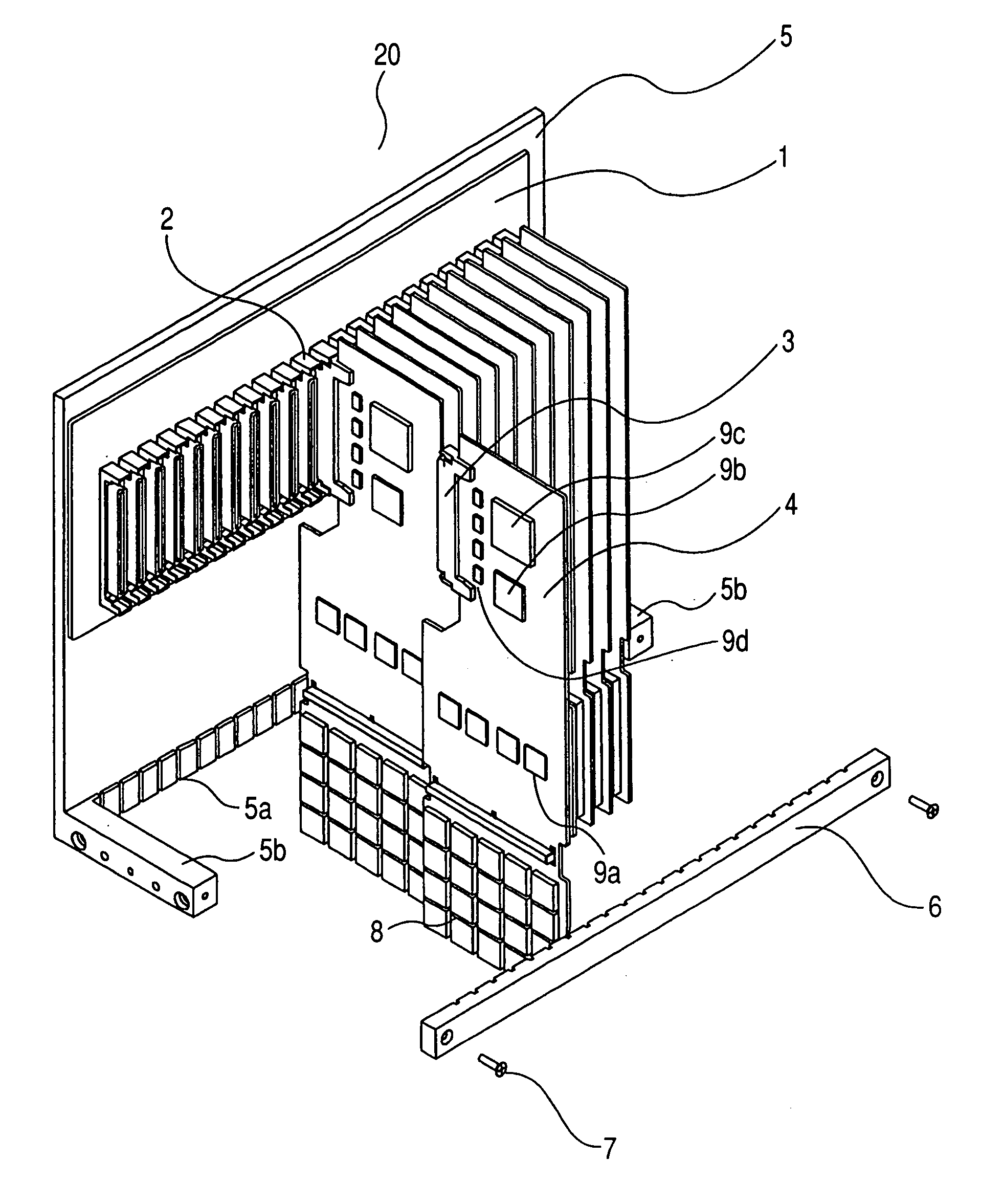
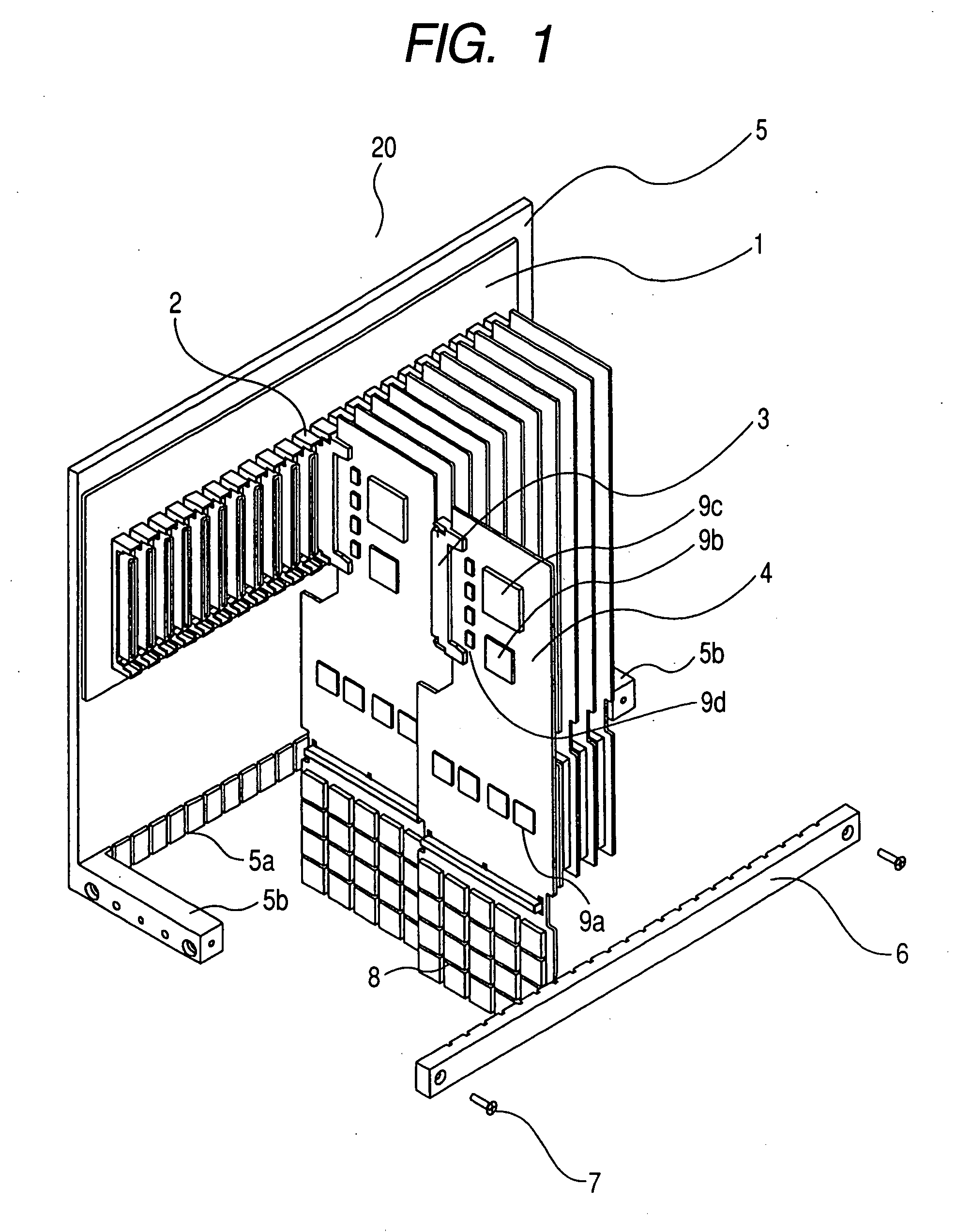
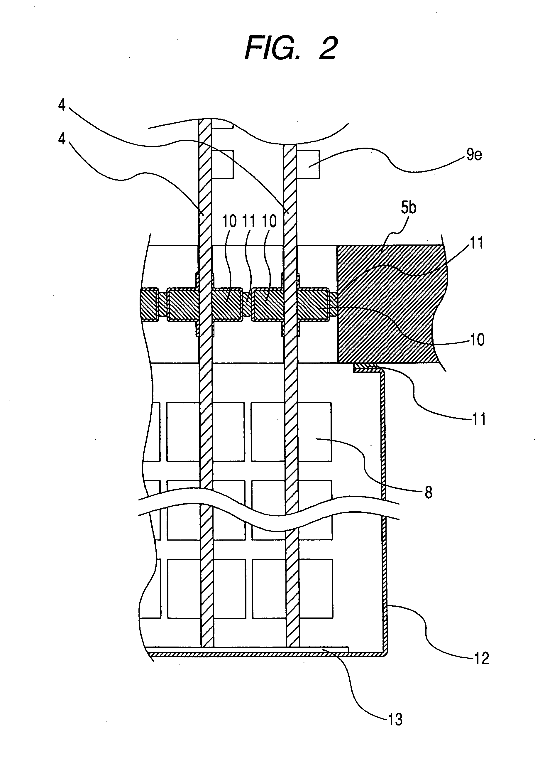
[0022] The structure for mounting a printed board according to a first embodiment of the present invention will be described with reference to FIGS. 1 through 3. FIG. 1 is a perspective view schematically illustrating the structure for mounting a printed board (the positioning of a printed board and the electromagnetic shielding structure thereof) according to the first embodiment of the present invention. FIG. 2 is a partially sectional view of a plurality of sub printed boards viewed from the board width direction, the plurality of sub printed boards being juxtaposed to one another in the structure for mounting a printed board according to the first embodiment of the present invention. FIG. 3 is a diagram of a sub printed board viewed from the element mounting side, the sub printed board being based on the structure for mounting a printed board according to the first embodiment of the present invention.

[0023]FIG. 1 partially illustrates electronic apparatus in which a multiplicit...

second embodiment

[0032] Next, a second embodiment of a nuclear medicine diagnosis system (for example, a PET system or a SPECT system), which has the structure for mounting a printed board according to the present invention, will be described with reference to FIG. 1.

[0033] The nuclear medicine diagnosis system (for example, a PET system or a SPECT system) according to the present invention includes: the sub printed board described in the first embodiment, which corresponds to the joint substrate described in JP-A-2005-106805 (the patent document 3); and the main printed board 1 described in the first embodiment, which is used as a top plate in this embodiment.

[0034]FIG. 1 is a diagram illustrating a basis configuration of an observation unit (detector unit) 20 that forms a camera in the PET system and the SPECT system. As a nuclear medicine diagnosis system, the PET system includes a camera (imaging unit), a data processor, and a display unit. A subject is imaged by use of the camera with the sub...


PUM


Abstract

The present invention is provided a structure for mounting a printed board in which each connector that is attached to each of a plurality of sub printed boards, which are juxtaposed to one another with respect to a main printed board secured to a metal backboard, is inserted into each of a plurality of connectors that are juxtaposed to one another on the main printed board so that the sub printed boards are mounted on the main printed board by the connector connections. Parts of both ends of an area in proximity to a semiconductor-device mounted area on each of the sub printed boards ate pinched between a first metal frame and a second metal frame so that each of the sub printed boards are secured.

Description

BACKGROUND OF THE INVENTION [0001] The present invention relates to a structure for mounting a printed board, in which a multiplicity of printed boards (sub substrates), which are juxtaposed to each other, are connected and mounted to a main printed board that is secured to a backboard, each of the printed boards including an electronic part area on which a plurality of electronic parts are mounted, and a semiconductor device area on which a plurality of semiconductor devices are mounted. The present invention also relates to an electronic apparatus (for example, a nuclear medicine diagnosis system having an observation unit such as a PET (Positron Emission Tomography) system and a SPECT (Single Photon Emission Computer Tomography) system) having the structure for mounting a printed board. [0002] Conventional structures for mounting a printed board are known by JP-A-2001-7572 (patent document 1) and JP-A-11-186708 (patent document 2). According to the patent document 1, when a plura...

Claims


Application Information

Patent Timeline
Patent Type & Authority Applications(United States)
IPC IPC(8): H02B1/00
CPCH05K1/14H05K7/1408H05K2201/2018H05K2201/044H05K9/0062
Inventor SHIMOIRISA, TAKAHIROKAWATA, ATSUMIKOZAWA, FUSAAKI
Owner HITACHI LTD
Why Eureka
Try Eureka